Method of forming pattern using fine pitch hard mask

a technology of hard mask and pattern, applied in the direction of semiconductor/solid-state device manufacturing, basic electric elements, electric apparatus, etc., can solve the problems of increasing difficulty in forming sufficiently fine patterns, difficult to remove spacer patterns, and general non-uniform thickness of each one of a paired set of spacers formed on the sidewalls of a particular pattern, etc., to achieve the effect of overcomplicating resolution limitations

Active Publication Date: 2007-05-31
SAMSUNG ELECTRONICS CO LTD
View PDF10 Cites 409 Cited by
  • Summary
  • Abstract
  • Description
  • Claims
  • Application Information

AI Technical Summary

Problems solved by technology

As the design rules for semiconductor devices have rapidly shifted towards micronization, it has become increasingly difficult to form sufficiently fine pitch patterns due to the resolution limitations of conventional photolithography processes used to form the patterns.
However, if this type of spacer pattern is used as the hard mask, the thickness of each one of a paired set of spacers formed on sidewalls of a particular pattern will generally be non-uniform.
This thickened spacer also makes it difficult to remove the spacer pattern after the spacer pattern is used as the hard mask.
This requirement further complicates the process of fabricating semiconductor devices on substrates and tends to drive up the associated costs and risks of patterning errors.

Method used


Image

  • Method of forming pattern using fine pitch hard mask
  • Method of forming pattern using fine pitch hard mask
  • Method of forming pattern using fine pitch hard mask

Examples


Embodiment Construction

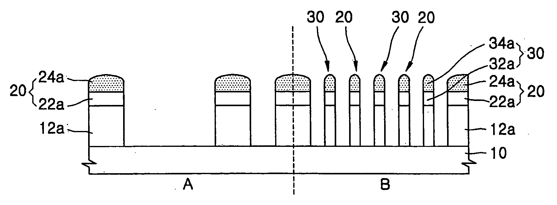
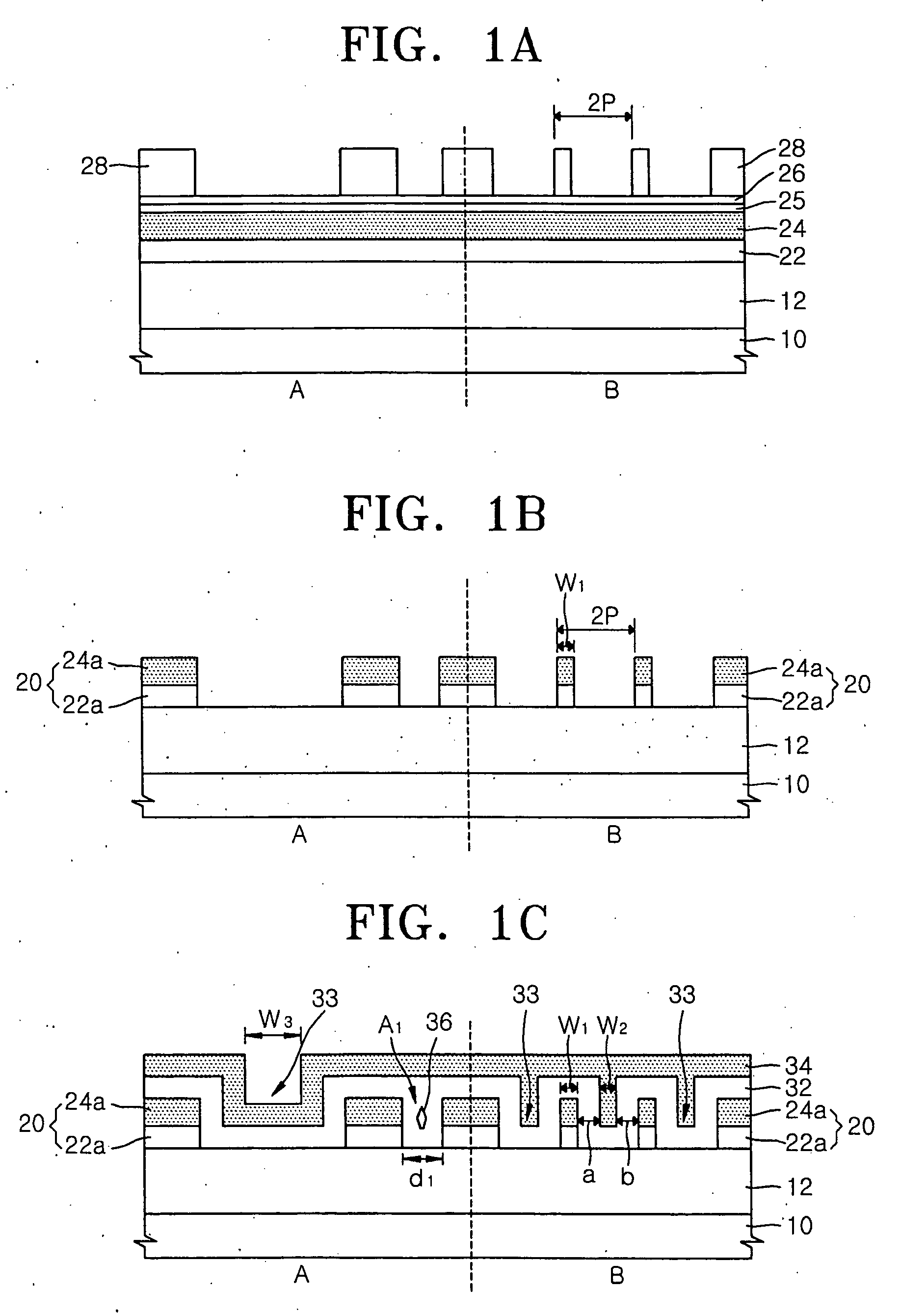
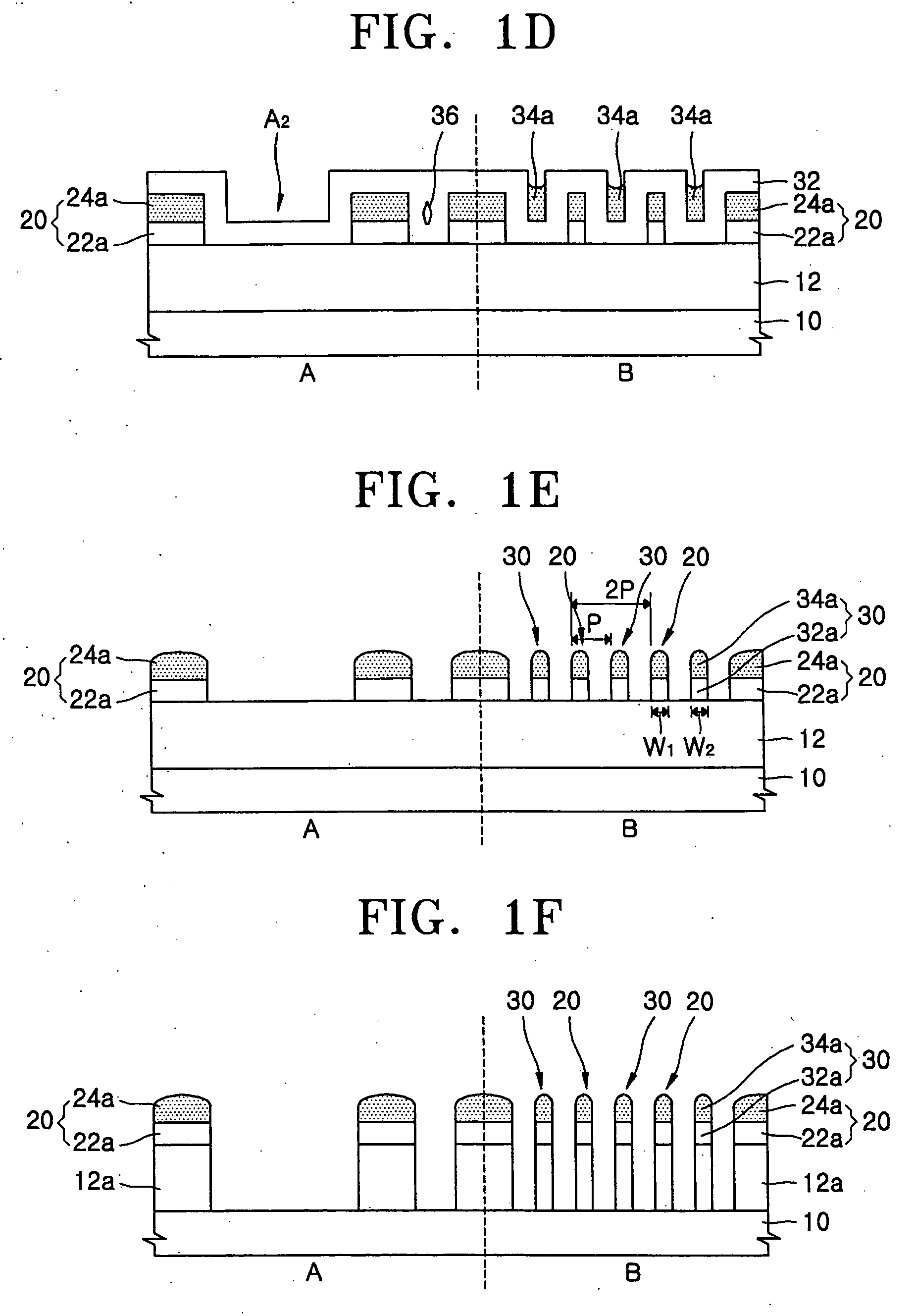
[0023]FIGS. 1A and 1F are cross-sectional views of an exemplary substrate on which fine patterns are formed using fine pitch hard mask patterns provided by one embodiment of the invention.

[0024] Referring to FIG. 1A, an etch target layer 12, a first mask layer 22 and a second mask layer 24 are sequentially formed on a substrate 10. The etch target layer 12 may be formed from various materials depending on the particular use of the patterns. For instance, when defining an active region on a semiconductor substrate, the etch target layer 12 may be formed of silicon. When forming a gate electrode, the etch target layer 12 may be formed of a conductive material, such as doped polysilicon or a stacked structure including doped polysilicon and a metal silicide. When forming a bit line, the etch target layer 12 may be formed of a metal or metal alloy, such as tungsten or aluminum.

[0025] The first mask layer 22 serves as a buffer for obtaining a uniform thickness of the second mask layer ...


PUM


Abstract

A method of forming a first hard mask pattern including a plurality of first line patterns formed on the etch target layer in a first direction and having a first pitch. A third layer is formed on sidewalls and an upper surface of the first hard mask pattern, such that the third layer includes a top surface having a recess formed between two adjacent first line patterns. A second hard mask pattern including a plurality of second line patterns each extending in the first direction within the recess is formed. Then, the third layer is anisotropically etched to selectively expose an etch target layer between the first line patterns and the second line patterns. Then, the etch target layer is anisotropically etched using the first hard mask pattern and the second hard mask pattern as an etch mask.

Description

STATEMENT OF RELATED APPLICATION(S) [0001] This application is a continuation in part of U.S. application Ser. No. 11 / 367,437 filed Mar. 6, 2006, which in turn claims the benefit of Korean Patent Application No. 10-2005-0032297 filed on Apr. 19, 2005. The subject matter of these related applications is hereby incorporated by reference.BACKGROUND OF THE INVENTION [0002] 1. Field of the Invention [0003] Embodiments of the invention relate to a method of fabricating a semiconductor device. More particularly, embodiments of the invention relate to a method of forming a fine pattern on a substrate using a fine pitch hard mask. [0004] 2. Description of Related Art [0005] Large scale integration of semiconductor devices has generally required the use of micronized patterns. Individual devices must be micronized in order to integrate a great multiplicity of devices within a limited area. As a result, it is commonly necessary to scale down the pitch of various patterns used to form the devic...

Claims


Application Information

Patent Timeline
Patent Type & Authority Applications(United States)
IPC IPC(8): H01L21/4763
CPCH01L21/0337H01L21/0338H01L21/32139H01L21/308
Inventor LEE, JI-YOUNGLEE, HAK-SUNKIM, MYEONG-CHEOLJEON, KYUNG-YUB
Owner SAMSUNG ELECTRONICS CO LTD
Why Eureka
Try Eureka