Chip package structure

a chip and package technology, applied in the direction of electrical equipment, semiconductor devices, semiconductor/solid-state device details, etc., can solve the problems of inconvenience and drawbacks in practical use of the above-mentioned chip package structure poor heat conduction efficiency of the heatsink, etc., to achieve improved chip package structure, and improved heat conduction efficiency

Inactive Publication Date: 2007-06-14
NIKO SEMICON
View PDF3 Cites 2 Cited by
  • Summary
  • Abstract
  • Description
  • Claims
  • Application Information

AI Technical Summary

Benefits of technology

[0007] An object of the present invention is to provide an improved chip package structure, in which a heat spreader is disposed in a package body and contacts a chip carrier so that heat generated by a chip can be transmitted to the heat spreader. The heat spreader is partially exposed out of the package body to discharge heat generated by the heat to a heatsink so as to discharge heat generated by the heat to the outside. Therefore, the heat conduction efficiency is better, and the heat spreading efficiency can be effectively enhanced.

Problems solved by technology

Therefore, the heat conduction efficiency is poor, resulting in a bad heat spreading efficiency of the heatsink.
Accordingly, the above prior art chip package structure has inconvenience and drawbacks in practical use.

Method used


Image

  • Chip package structure
  • Chip package structure
  • Chip package structure

Examples


Embodiment Construction

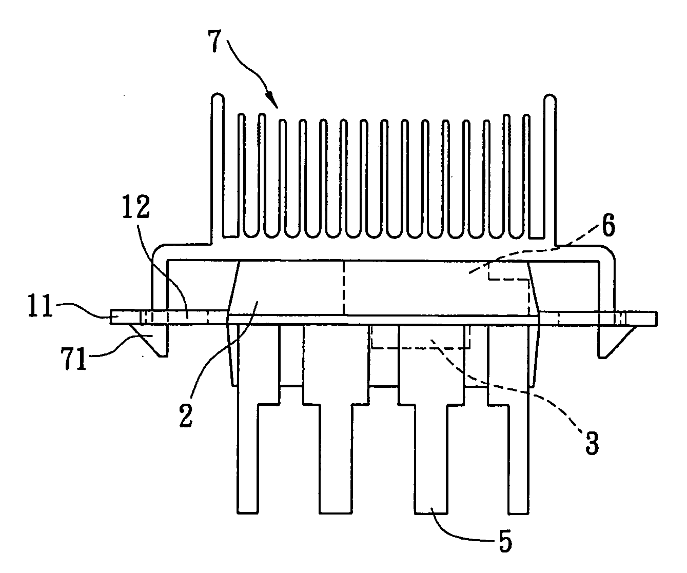
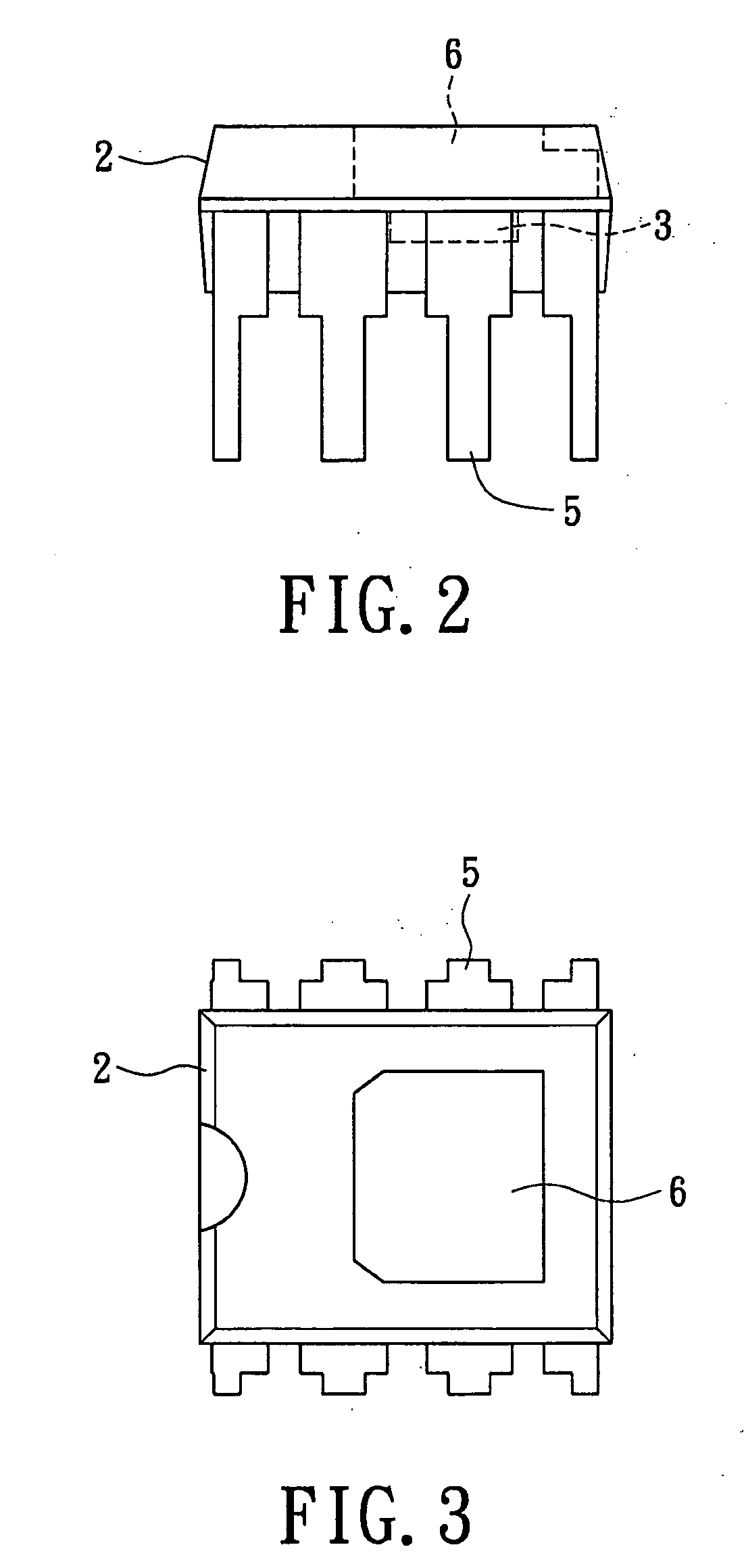
[0017] As shown in FIGS. 2 to 5, the present invention provides an improved chip package structure, which at least comprises a chip carrier 1 and a package body 2. The chip carrier 1 is a metal piece made of metal material. At least a chip 3 is adhered and fixed onto the bottom surface of the chip carrier 1. A plurality of leads 4 are then used to electrically connect the chip 3 and a plurality of pins 5 by means of wire bonding. The package body 2 is packaged around the chip carrier 1, the chip 3 and the leads 4 to seal the chip carrier 1, the chip 3 and the leads 4 therein. The pins 5 are disposed at two opposite sides of the package body 2 and extend beyond the package body 2.

[0018] A heat spreader 6 is disposed in the package body 2. The heat spreader 6 is made of metal material with good heat conductivity. The heat spreader 6 is fixed in the package body 2. The bottom face of the heat spreader 6 contacts the chip carrier 1. The heat spreader 6 has a partially exposed portion (...


PUM


Abstract

An improved chip package structure includes a chip carrier, a chip, a plurality of pins, a plurality of leads, a package body and a heat spreader. The chip is fixed on the chip carrier. The leads are electrically connected between the chip and the pins. The package body is packaged outside the chip carrier, the chip and the leads. The heat spreader is disposed in the package body. The heat spreader contacts the chip carrier, and is partially exposed out of a face (top face) of the package body. Heat generated by the chip can thus be transmitted to a heatsink via the chip carrier and the heat spreader so as to discharge a large amount of heat generated by the chip to the outside. The improved chip package structure has a good heat conduction efficiency and an effectively enhanced heat spreading efficiency.

Description

BACKGROUND OF THE INVENTION [0001] 1. Field of the invention [0002] The present invention relates to an improved chip package structure and, more particularly, to an improved chip package structure, which can discharge a large amount of heat generated by a chip to the outside, and has a good heat conduction efficiency and an effectively enhanced heat spreading efficiency. [0003] 2. Description of Related Art [0004] In a prior art chip package structure, a chip is adhered onto a chip carrier, and leads are used to electrically connect the chip on the chip carrier to pins by means of wire bonding. Packaging is then performed to form a package body with the chip carrier, the chip and the leads sealed therein. As shown in FIG. 1, a package body 8 is formed outside a chip package structure, and two lines of pins 9 are formed at two opposite sides of the package body 8. [0005] With the swift development of the computer industry, the execution speed of chip becomes faster and faster, and h...

Claims


Application Information

Patent Timeline
Patent Type & Authority Applications(United States)
IPC IPC(8): H01L23/495
CPCH01L23/4093H01L23/49562H01L23/49575H01L2224/48137H01L2224/48247H01L2224/49171H01L24/48H01L24/49H01L2924/00H01L2924/181H01L2924/00014H01L2924/00012H01L2224/45099H01L2224/45015H01L2924/207
Inventor TSAI, FAN
Owner NIKO SEMICON
Why Eureka
Try Eureka