Integrated circuit chip with external pads and process for fabricating such a chip
- Summary
- Abstract
- Description
- Claims
- Application Information
AI Technical Summary
Problems solved by technology
Method used
Image

Examples
Embodiment Construction
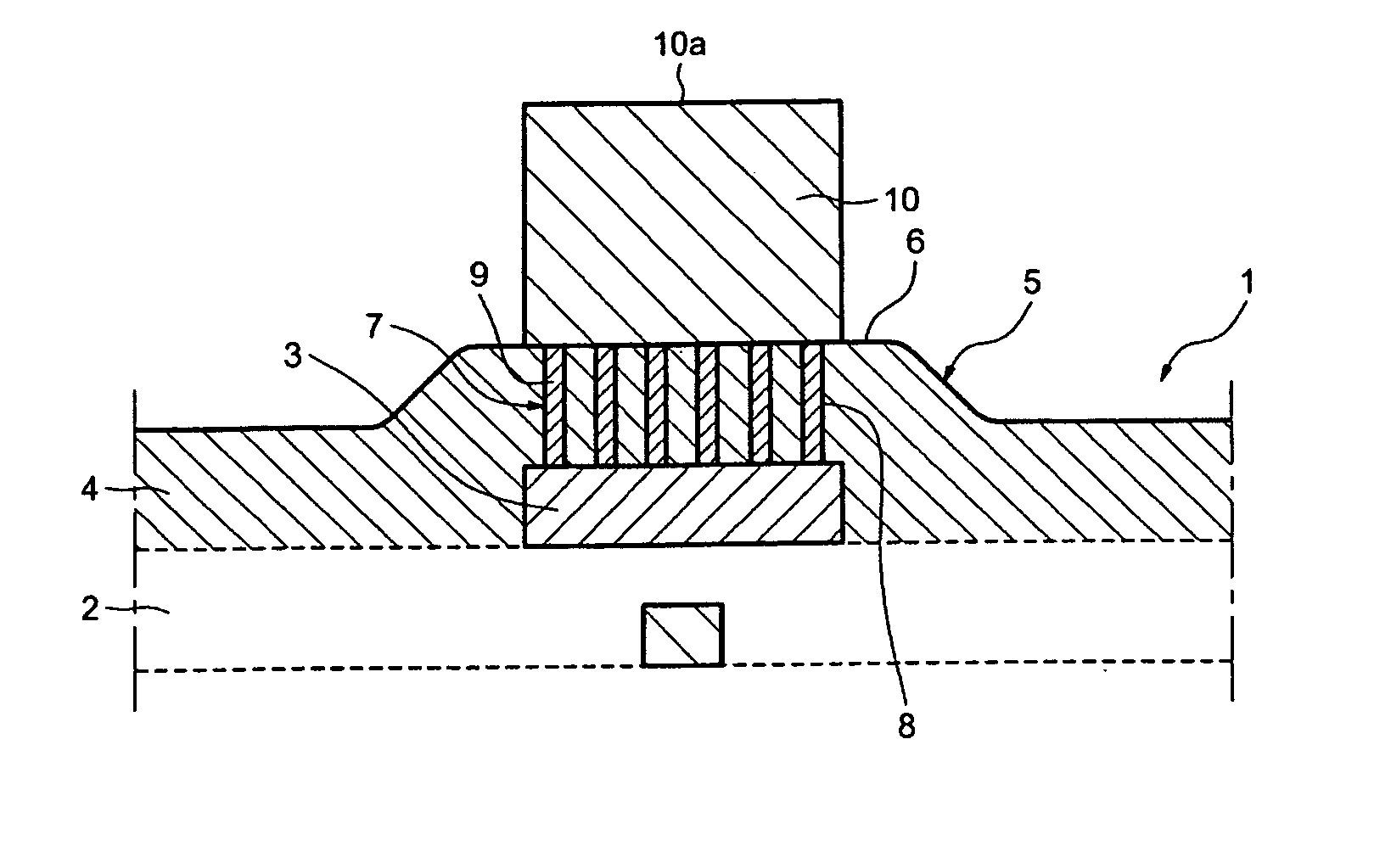
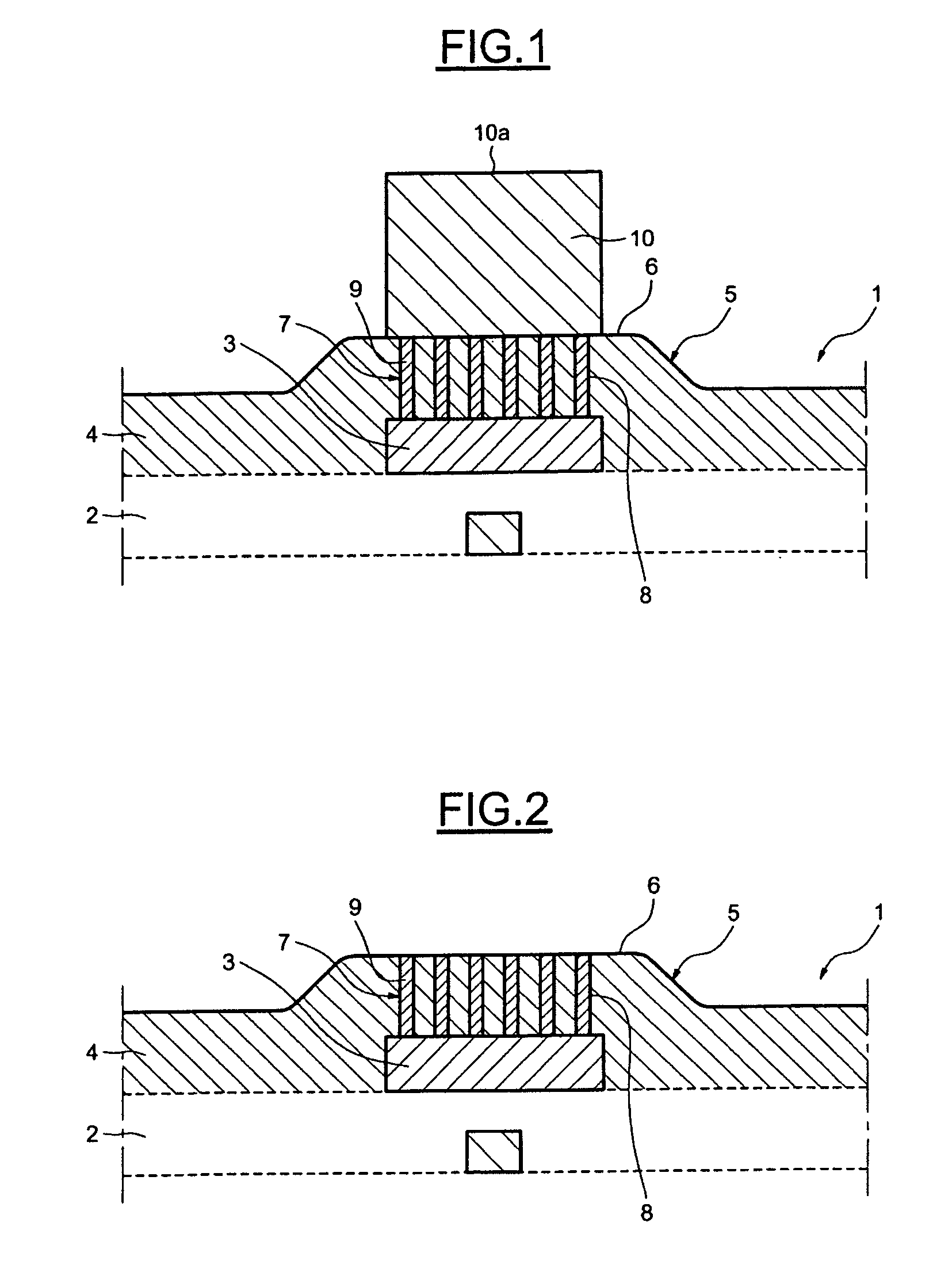
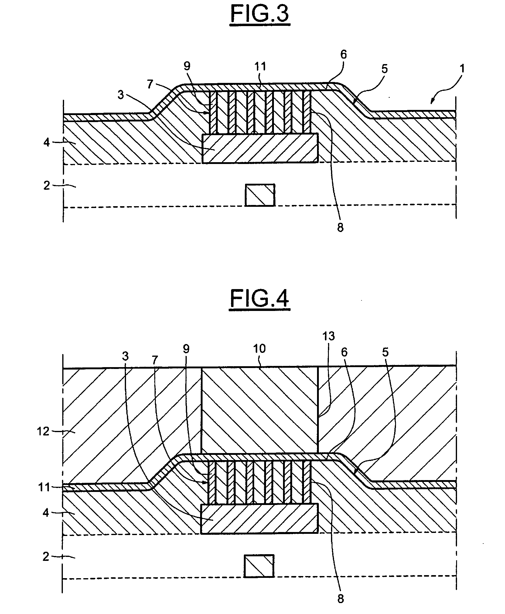
[0019] Referring to FIG. 1, it may be seen that an integrated circuit chip 1 is made up of several successive layers, which includes a final layer 2 on which are formed spaced-apart metal internal pads 3 and, on this final layer 2, a dielectric surface layer 4 called a passivation layer, this surface layer 4 having bumps 5 that envelop, via the top, the internal pads 3 and have a flat front face 6. Of course, the internal pads 3 are selectively connected to the integrated circuits.
[0020] Provided in the surface layer 4 are multiplicities 7 of holes 8 formed respectively above the internal pads 3, the holes 8 of each multiplicity 7 being preferably distributed in the form of regular matrices below the flat front face 6.
[0021] Vias 9 made of an electrically conducting material are formed in the holes 8.
[0022] Formed on the flat front faces 6 of the bumps 5 of the surface layer 4 are projecting external contact pads 10 made of an electrically conducting material, for example of para...
PUM
 Abstract
Description
Claims
Application Information
 - R&D
- Intellectual Property
- Life Sciences
- Materials
- Tech Scout
- Unparalleled Data Quality
- Higher Quality Content
- 60% Fewer Hallucinations
Browse by: Latest US Patents, China's latest patents, Technical Efficacy Thesaurus, Application Domain, Technology Topic, Popular Technical Reports.
© 2025 PatSnap. All rights reserved.Legal|Privacy policy|Modern Slavery Act Transparency Statement|Sitemap|About US| Contact US: help@patsnap.com