Liquid-crystal display device
a display device and liquid crystal technology, applied in static indicating devices, non-linear optics, instruments, etc., can solve problems such as visual degradation
- Summary
- Abstract
- Description
- Claims
- Application Information
AI Technical Summary
Benefits of technology
Problems solved by technology
Method used
Image
Examples
first embodiment
[0023] Referring now to FIGS. 1 to 6, the LCD device 10 according to a first embodiment of the present invention will be described. The LCD device 10 in this embodiment is a normally-white OCB-mode LCD device.
(1) Structure of Display Panel 12 in Thickness-Wise Cross Section
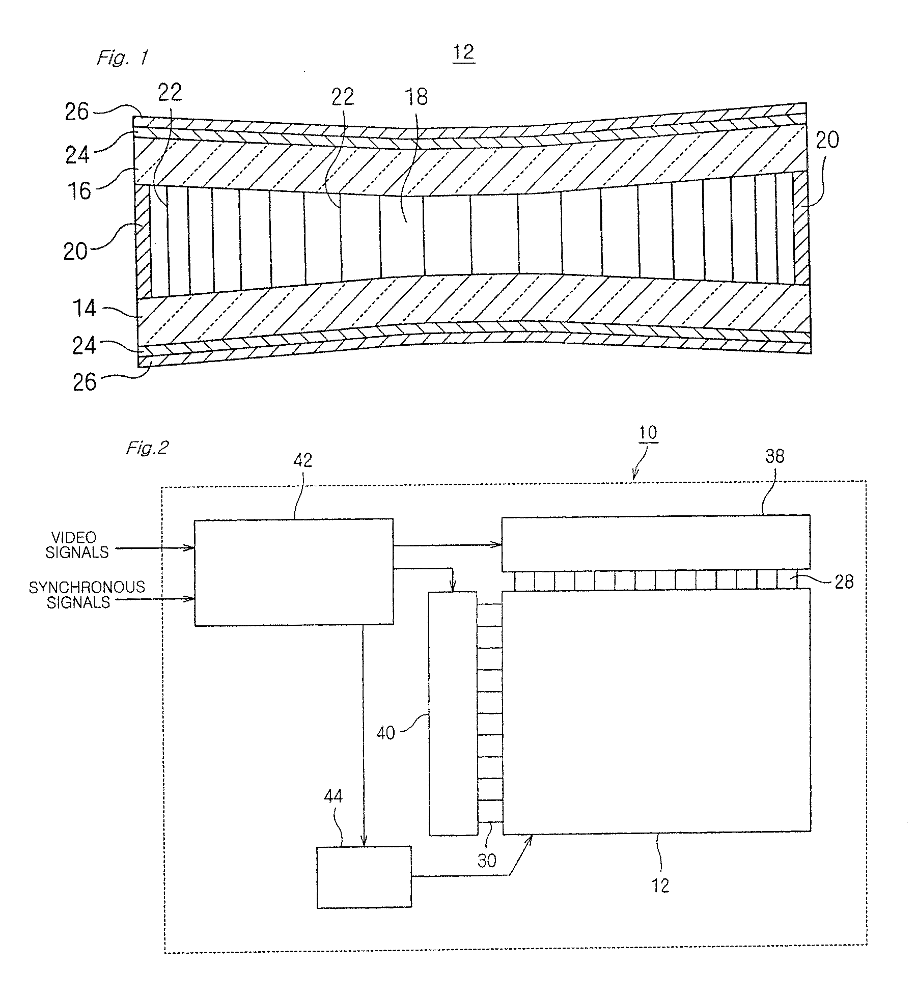
[0024] Referring now to FIG. 1, a structure of a display panel 12 of the LCD device 10 in thickness-wise cross section will be described. The LCD device 10 has a viewing area that is surrounded by a pattern of a sealing material 20 and has a diagonal dimension of 32 inches.
[0025] An array substrate 14 and a counter substrate 16, each of which is formed of an insulator substrate such as a glass plate and has an inner face having electrode (s), are arranged as overlaid to sandwich a layer 18 of liquid-crystal material for the OCB mode. All-around periphery of the display panel 12 is sealed by the sealing material 20, at between the array substrate 14 and the counter substrate 16. The thickness of the liquid crys...
second embodiment
[0053] Referring now to FIG. 9 to FIG. 11, a second embodiment of the present invention will be described.
[0054] In the first embodiment, the retardation of the display panel in the display area is increased gradually from an optimal value from the central portion to the end portion by differentiating the cell gap between the central portion and the end portion of the viewing area.
[0055] Alternatively, in the second embodiment, the substantially equivalent advantageous effect as the first embodiment is achieved by adjusting a range of voltage applied at pixels, which is outputted to the pixels corresponding to video signal supplied from the outside.
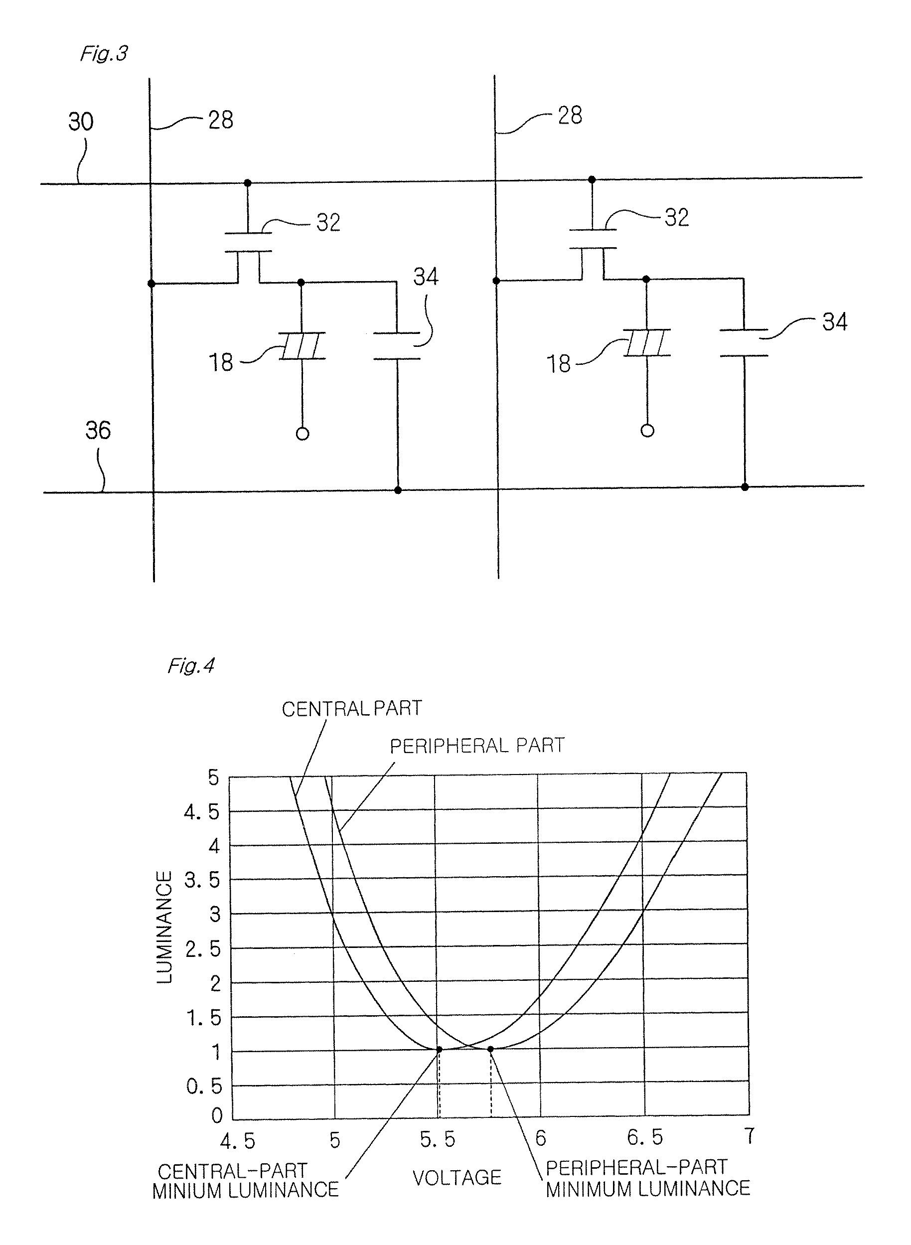
[0056] In other words, the voltage range is separately set for each region of the viewing area; so that luminance on pixels in the central portion becomes substantially the minimum luminance at the time of black-displaying; and so that the luminance of each pixel monotonously decreases within the voltage range even though there are var...
third embodiment
[0068] A third embodiment of the invention will be described.
[0069] In the third embodiment, the same advantageous effect as the above-described embodiments is achieved by varying extents of the retardation of the retardation films, such as half or quarter wave plates, which are attached respectively to regions of the viewing area on of the display panel.
[0070] For example, the advantageous effect as the above is achieved by setting the retardation of the retardation plate for the regions A, B and C in FIG. 9, as follows; 60 nm for the central region A, 57 nm for the intermediate region B, and 56 nm for the end region C.
[0071] Such a retardation adjustment is achieved when consecutively attached in following order are; a first retardation plate covering whole of the viewing area; a second retardation plate covering the intermediate region B and the central region C; and third retardation plate only covering the central region C. In this embodiment as well, the above-described man...
PUM
 Abstract
Description
Claims
Application Information


