Plasma display panel and display device using the same
a technology of display panel and display device, which is applied in the direction of static indicating device, discharge tube luminescnet screen, instruments, etc., can solve the problems of unnecessary light emission, significant reduction luminance (minimum luminance) of the minimum luminance, etc., to improve the dark-room contrast, improve the display performance of a pdp, and improve the contras
- Summary
- Abstract
- Description
- Claims
- Application Information
AI Technical Summary
Benefits of technology
Problems solved by technology
Method used
Image
Examples
first embodiment
[0048]Such a case is described that the present embodiment is applied to a PDP of 50 inch full HD (1920×1080 pixels). In this case, a cell pitch thereof is 580 μm long and 192 μm wide.
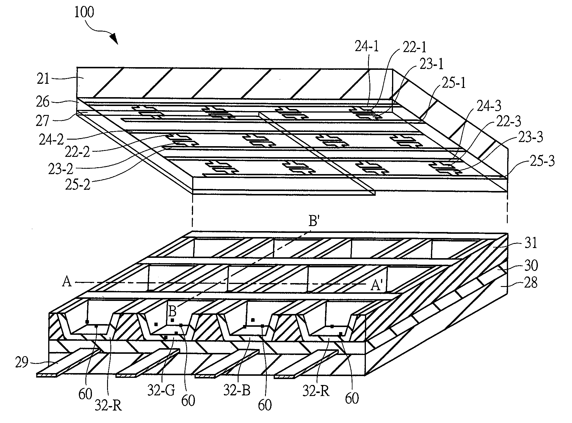
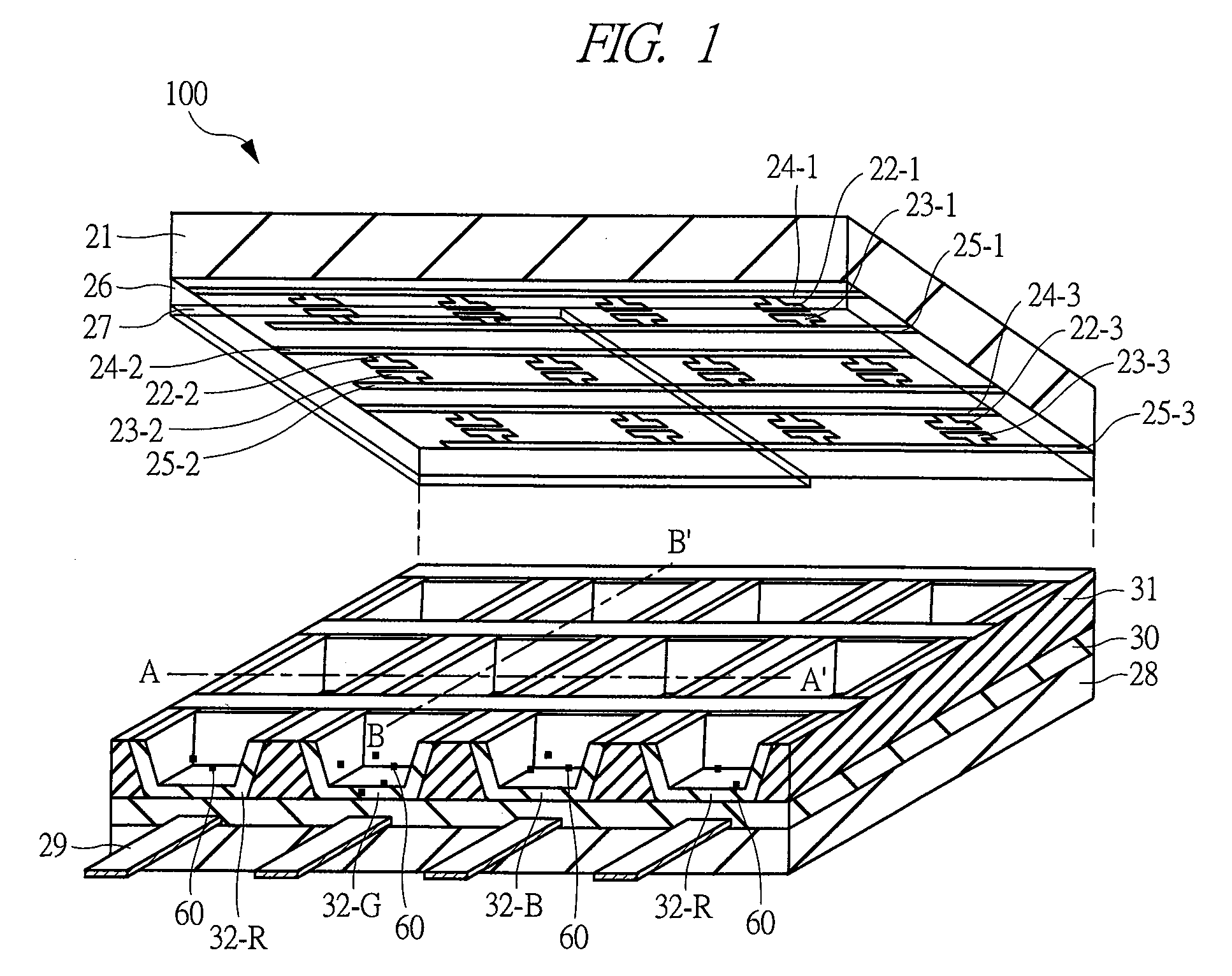
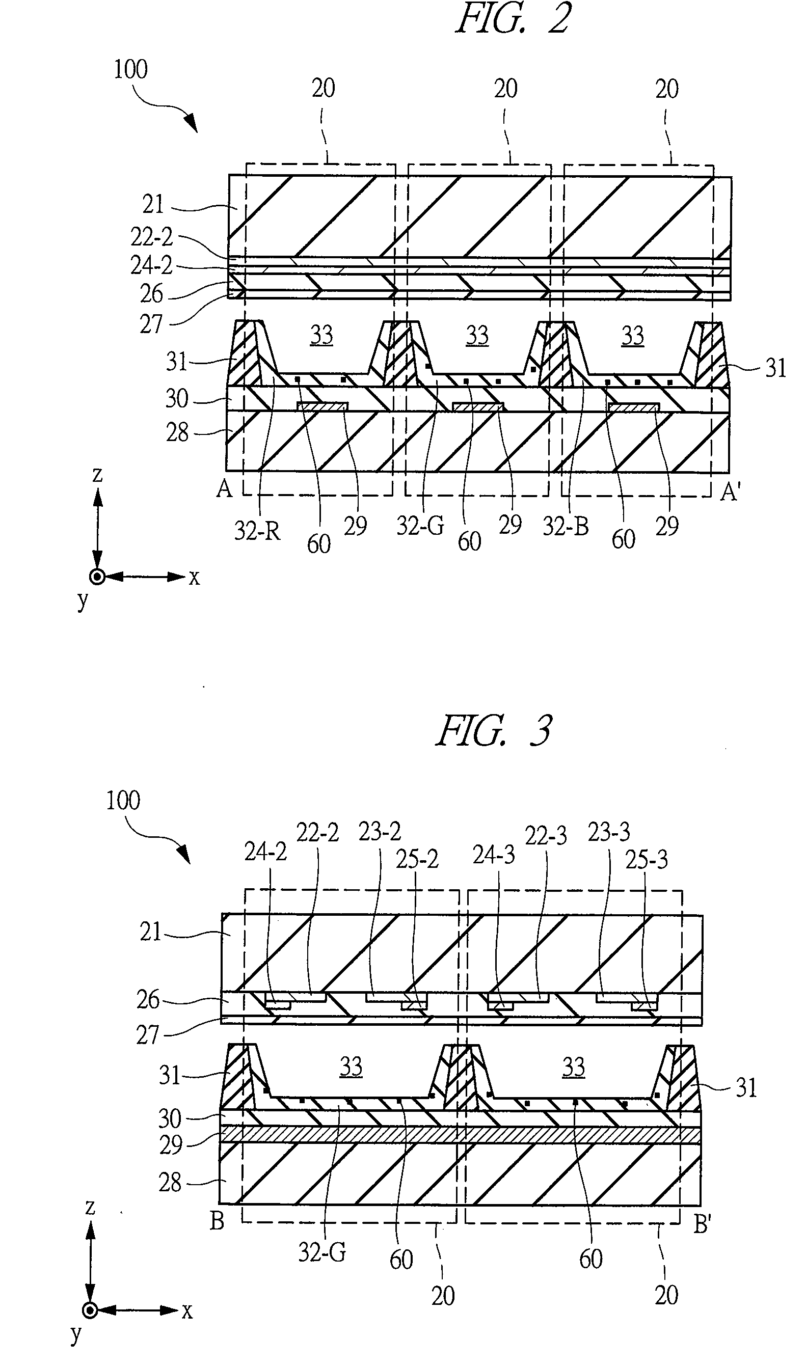
[0049]FIG. 1 is a perspective view schematically showing a principal part of a PDP 100 according to the present embodiment, FIG. 2 is a cross-sectional view taken along the line A-A′ of FIG. 1, and FIG. 3 is a cross-sectional view taken along the line B-B′ of FIG. 1. Although a front substrate 21 is illustrated so as to be away from a back substrate 28 in the PDP 100 shown in FIGS. 1 to 3 for easily understanding its configuration, the front substrate 21 and the back substrate 28 are attached to be combined so as to face each other in their thickness direction (z direction). Also, in FIG. 1, a dielectric layer 26 and a protective film 27 are illustrated in a perspective manner, and further, the protective film 27 is illustrated in a partly-missing manner.
[0050]The PDP 100 has a configuration in which t...
second embodiment
[0103]In the first embodiment, the minimum luminance can be reduced by adjusting the amount of the crystal material (for example, MgO crystal) having the large secondary electron emission coefficient and the large charged amount and mixing the crystal material into the phosphor of each color so as to uniform the weak discharge firing voltages. However, when the crystal material is mixed too much, the phosphor amount is reduced, and therefore, the reduction of the luminance is considered. Accordingly, in a second embodiment, a PDP using the crystal material arranged in the phosphor layers with considering the luminance of the PDP will be described. Note that descriptions overlapped with those of the first embodiment are omitted.
[0104]FIG. 14 is a diagram showing a relation between the mixture concentration of the MgO crystal and a panel luminance. It is found that the luminance is lowered to 9% when the MgO mixture concentration is 20%, and further, the luminance is lowered to 13% wh...
PUM
 Abstract
Description
Claims
Application Information


