Organic light emitting display and method of fabricating the same

a technology of light-emitting display and organic materials, which is applied in the direction of discharge tube luminescnet screens, discharge tube/lamp details, electric discharge lamps, etc., can solve the problems of large-sized screens, large power consumption, and complex manufacturing processes,

Active Publication Date: 2007-07-26
SAMSUNG DISPLAY CO LTD
View PDF99 Cites 87 Cited by
  • Summary
  • Abstract
  • Description
  • Claims
  • Application Information

AI Technical Summary

Benefits of technology

[0014]In the above described method, interposing may comprise contacting the frit with the portion of the electrically conductive line and the second substrate. The unfinished device may further comprise a planarization layer generally formed over the electrically conductive line with an opening exposing part of the conductive line, and wherein interposing the frit comprises contacting the frit with the electrically conductive line through the opening. Providing the unfinished device may further comprise providing the planarization layer over the electrically conductive line, and selectively etching the planarization layer to form the opening. The melting may comprise irradiating a laser beam or infrared ray to at least part of the frit. The interposing of the frit may comprise forming the frit over at least one of the first and second substrates, and arranging the first and second substrate so as to interpose the frit therebetween. Forming the

Problems solved by technology

Since the liquid crystal display is a passive device rather than an emissive device, it is difficult to make having high brightness and contrast, a wide viewing angle,

Method used


Image

  • Organic light emitting display and method of fabricating the same
  • Organic light emitting display and method of fabricating the same
  • Organic light emitting display and method of fabricating the same

Examples


Embodiment Construction

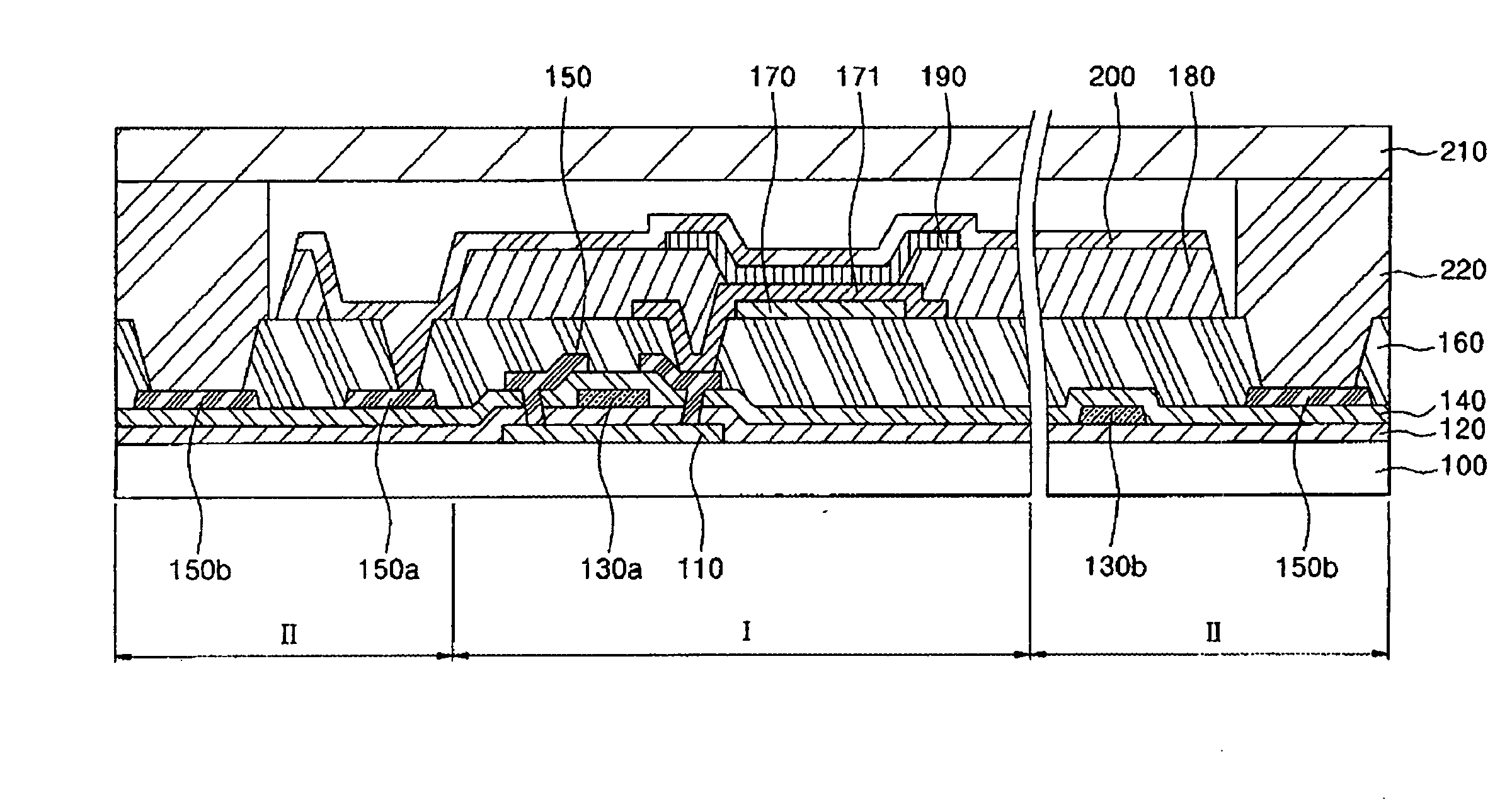
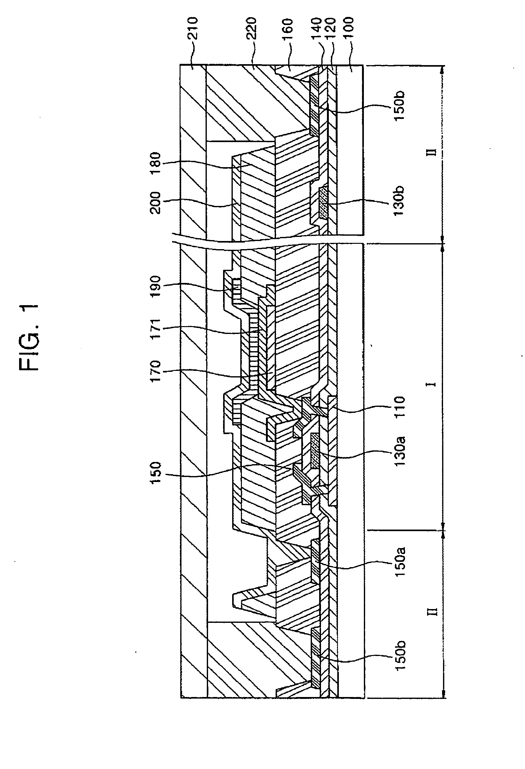
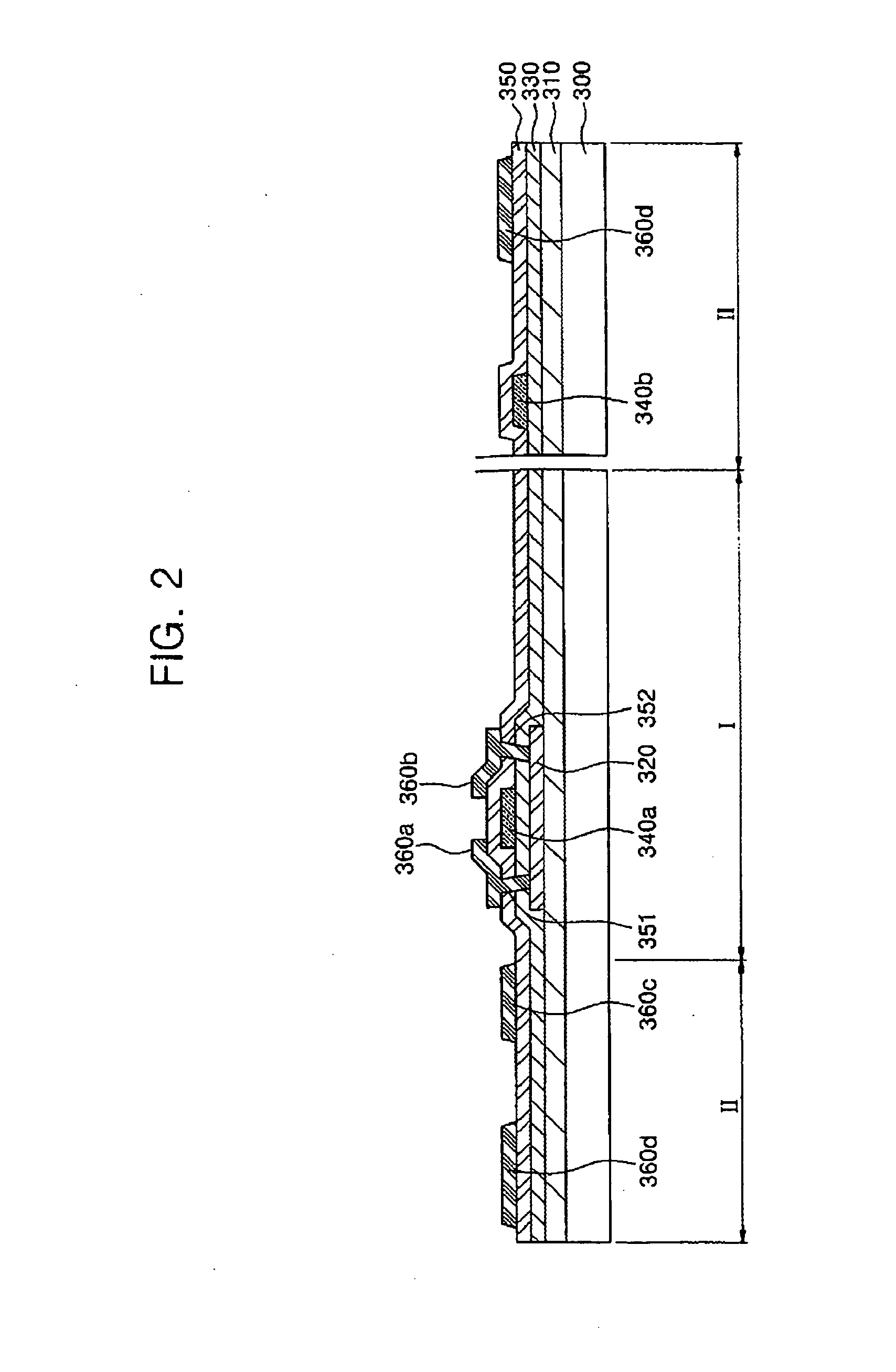
[0025]The present invention will now be described more fully hereinafter with reference to the accompanying drawings, in which some embodiments of the invention are shown. This invention may, however, be embodied in different forms and should not be construed as limited to the embodiments set forth herein. Rather, these embodiments are provided so that this disclosure will be thorough and complete, and will fully convey the scope of the invention to those skilled in the art. In the drawings, the thickness of layers and regions may be exaggerated for clarity. Like reference numerals designate like elements throughout the specification.

[0026]An organic light emitting display (OLED) is a display device comprising an array of organic light emitting diodes. Organic light emitting diodes are solid state devices which include an organic material and are adapted to generate and emit light when appropriate electrical potentials are applied.

[0027]OLEDs can be generally grouped into two basic ...


PUM


Abstract

Disclosed are an organic light emitting display and a method of fabricating the same that are capable of preventing deterioration of adhesive strength of a glass frit for sealing a substrate. An organic light emitting device according to one embodiment of the present invention includes a first substrate including a pixel region and a non-pixel region, an array of organic light emitting pixels formed over the pixel region of the first substrate, and a second substrate placed over the first substrate, the array being interposed between the first and second substrates. The organic light emitting device of this embodiment further includes an electrically conductive line formed over the non-pixel region of the first substrate, and a frit seal interposed between the first and second substrates and surrounding the array such that the array is encapsulated by the first substrate, the second substrate and the frit seal, wherein the electrically conductive line comprises a portion overlapping the frit seal in a segment of the device such that the portion of the electrically conductive line substantially eclipses the frit seal when viewed from the first substrate.

Description

CROSS-REFERENCE TO RELATED APPLICATIONS[0001]This application claims priority to and the benefit of Korean Patent Application Nos. 10-2006-0007962, filed Jan. 25, 2006, and 10-2006-0027321, filed Mar. 27, 2006, the disclosures of which are incorporated herein by reference in their entirety. This application is related to and incorporates herein by reference the entire contents of the following concurrently filed applications:ApplicationTitleAtty. Docket No.Filing DateNo.ORGANIC LIGHT-EMITTING DISPLAYSDISHN.043AUSDEVICE AND METHOD OFFABRICATING THE SAMEORGANIC LIGHT-EMITTING DISPLAYSDISHN.045AUSDEVICE AND METHOD OFMANUFACTURING THE SAMEORGANIC LIGHT EMITTING DISPLAYSDISHN.048AUSDEVICEORGANIC LIGHT-EMITTING DISPLAYSDISHN.051AUSDEVICE WITH FRIT SEAL ANDREINFORCING STRUCTUREORGANIC LIGHT EMITTING DISPLAYSDISHN.052AUSDEVICE METHOD OF FABRICATINGTHE SAMEORGANIC LIGHT EMITTING DISPLAYSDISHN.053AUSAND METHOD OF FABRICATING THESAMEORGANIC LIGHT-EMITTING DISPLAYSDISHN.054AUSDEVICE WITH FRIT S...

Claims


Application Information

Patent Timeline
IPC IPC(8): H05B33/04
CPCH01L27/3276H01L51/5246H01L27/3288H10K59/179H10K59/131H10K50/8426
Inventor CHOI, DONG SOOPARK, JIN WOO
Owner SAMSUNG DISPLAY CO LTD
Why Eureka
Try Eureka