
Organic light emitting display device and method of fabricating the same

a light-emitting display and organic technology, applied in the direction of luminescnet screens, instruments, discharge tubes, etc., can solve the problems of consuming more power, lcd has technical limits in brightness, contrast, viewing angle, size, etc., and is more complex to manufacture in comparison with other fpds

Active Publication Date: 2007-07-26
SAMSUNG DISPLAY CO LTD
View PDF75 Cites 77 Cited by
  • Summary
  • Abstract
  • Description
  • Claims
  • Application Information

AI Technical Summary

Benefits of technology

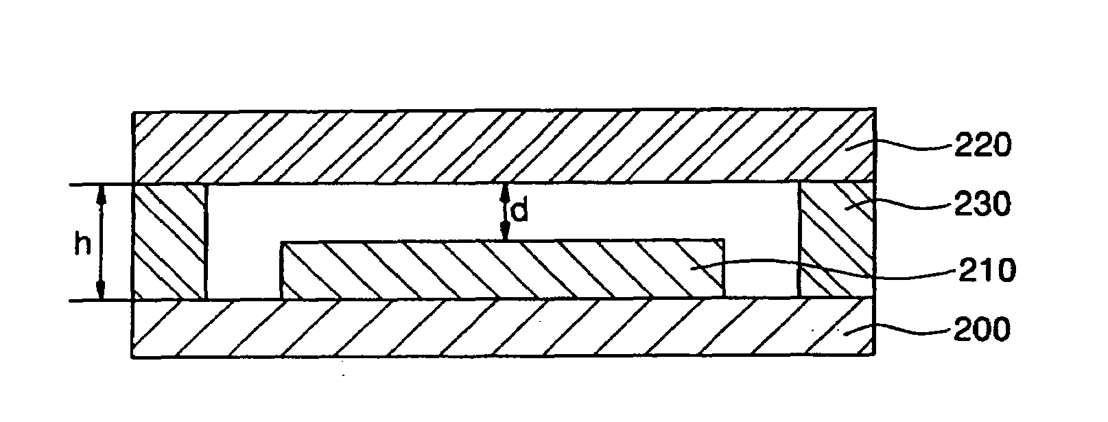
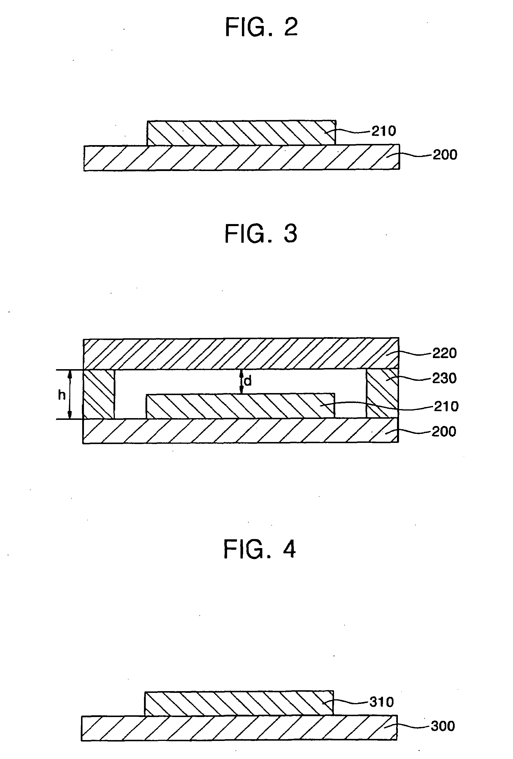
[0008]In the foregoing device, the gap distance may be about 10 to about 300 μm. The gap distance may be from about 10 to about 100 μm. The gap distance may be from about 10 to about 30 μm. The array may be configured to emit visible light through the top surface. The height may be the shortest distance between the first and second substrates, wherein the height may be from about 10 to about 300 μm. The second substrate may comprise a display surface facing away from the first substrate and configured to display an image thereon, and wherein the device may be configured to display an image on the display surface substantially free of Newton's rings. The array may comprise a first electrode, a second electrode and at least one organic layer interposed therebetween, wherein the second electrode may be closer to the second substrate than the first electrode, and wherein the top surface may comprise a surface of the second electrode facing the second substrate. The array may comprise a first electrode, a second electrode and at least one organic layer interposed therebetween, wherein the second electrode may be closer to the second substrate than the first electrode, wherein the array may further comprise a substantially transparent layer formed on the second electrode, and wherein the top surface may comprise a surface of the substantially transparent layer which faces the second substrate. The gap may comprise an air gap. The gap may be substantially filled with a solid material. The frit seal may comprise one or more materials selected from the group consisting of magnesium oxide (MgO), calcium oxide (CaO), barium oxide (BaO), lithium oxide (Li2O), sodium oxide (Na2O), potassium oxide (K2O), boron oxide (B2O3), vanadium oxide (V2O5), zinc oxide (ZnO), tellurium oxide (TeO2), aluminum oxide (Al2O3), silicon dioxide (SiO2), lead oxide (PbO), tin oxide (SnO), phosphorous oxide (P2O5), ruthenium oxide (Ru2O), rubidium oxide (Rb2O), rhodium oxide (Rh2O), ferrite oxide (Fe2O3), copper oxide (CuO), titanium oxide (TiO2), tungsten oxide (WO3), bismuth oxide (Bi2O3), antimony oxide (Sb2O3), lead-borate glass, tin-phosphate glass, vanadate glass, and borosilicate.

Problems solved by technology

Since the LCD is a non-emissive device, the LCD has technical limits in brightness, contrast, viewing angle, and size.
Also, the PDP is an emissive display, but the PDP is heavier, consumes more power, and is more complex to manufacture in comparison with other FPDs.

Method used


Image

  • Organic light emitting display device and method of fabricating the same
  • Organic light emitting display device and method of fabricating the same
  • Organic light emitting display device and method of fabricating the same

Examples


example

[0068]FIG. 6 is a graph of luminance versus an air gap between a substrate and an encapsulation substrate. In FIG. 6, an abscissa denotes an air gap “d” between the top surface of an array at the central portions of a substrate on which the array of organic light emitting diodes is formed and an encapsulation substrate, which is expressed in nanometers (nm), and an ordinate denotes luminance of Newton's rings versus the air gap “d”. Referring to FIG. 6, it can be seen that as the air gap “d” between the substrate on which the organic light emitting diode is formed and the encapsulation substrate increases, variation in the intensity of the Newton's rings, which is shown as amplitude, gradually decreases. Further, when the air gap “d” between the substrate and the encapsulation substrate exceeds about 10000 nm (i.e., 10 μm), the amplitude becomes fine.

[0069]Specifically, light reflected on the encapsulation substrate interferes with light that passes through the encapsulation substra...


PUM


Abstract

Provided is an organic light emitting display device (OLED) for preventing Newton's rings to improve image quality. An organic light emitting display device according to one embodiment of the present invention comprises a first substrate comprising a single layer or multiple layers; a second substrate comprising a single layer or multiple layers, the second substrate comprising an inner surface facing the first substrate; an array of organic light emitting pixels formed on the first substrate and interposed between the first and second substrates, the array comprising a top surface opposing the inner surface of the second substrate, wherein the top surface and the inner surface has a gap therebetween, and the gap has a gap distance measured between the top surface and the inner surface; and a frit seal interconnecting the first and second substrates while surrounding the array, wherein the frit seal, the first substrate and the second substrate in combination define an enclosed space in which the array is located, wherein the frit seal has a height between the first and second substrates so as to form the gap distance equal to or greater than about 10 μm.

Description

CROSS-REFERENCE TO RELATED APPLICATION[0001]This application claims priority to and the benefit of Korean Patent Application No. 10-2006-0007963, filed Jan. 25, 2006, the disclosure of which is incorporated herein by reference in its entirety. This application is related to and incorporates herein by reference the entire contents of the following concurrently filed applications:ApplicationTitleAtty. Docket No.Filing DateNo.ORGANIC LIGHT-EMITTING DISPLAYSDISHN.043AUSDEVICE AND METHOD OFFABRICATING THE SAMEORGANIC LIGHT-EMITTING DISPLAYSDISHN.045AUSDEVICE AND METHOD OFMANUFACTURING THE SAMEORGANIC LIGHT EMITTING DISPLAYSDISHN.048AUSDEVICEORGANIC LIGHT-EMITTING DISPLAYSDISHN.051AUSDEVICE WITH FRIT SEAL ANDREINFORCING STRUCTUREORGANIC LIGHT EMITTING DISPLAYSDISHN.052AUSDEVICE METHOD OF FABRICATINGTHE SAMEORGANIC LIGHT EMITTING DISPLAYSDISHN.053AUSAND METHOD OF FABRICATING THESAMEORGANIC LIGHT-EMITTING DISPLAYSDISHN.054AUSDEVICE WITH FRIT SEAL ANDREINFORCING STRUCTURE BONDEDTO FRAMEMETHO...

Claims


Application Information

Patent Timeline
Patent Type & Authority Applications(United States)
IPC IPC(8): H01J1/62H01J63/04
CPCH01L27/3281H01L51/5281H01L51/5246H01L51/524H10K59/17H10K59/8791H10K59/871H10K59/8722G02F1/1303B08B3/041G02F1/1316H10K50/8426H10K50/86H10K50/841
Inventor CHOI, DONG-SOOPARK, JIN-WOOJEONG, HEE-SEONGPARK, HYUN-SOOK
Owner SAMSUNG DISPLAY CO LTD
Learn More