Integrated circuit with a very small-sized reading diode

a reading diode, integrated circuit technology, applied in the direction of basic electric elements, semiconductor/solid-state device manufacturing, electric devices, etc., can solve the problem that the diode places a lower limit on the size of the diode to be given

Inactive Publication Date: 2007-08-09
ATMEL GRENOBLE
View PDF8 Cites 37 Cited by
  • Summary
  • Abstract
  • Description
  • Claims
  • Application Information

AI Technical Summary

Benefits of technology

[0016] With this method, it is typically possible to produce a diode with dimensions of about 1.5 micrometer by 1.5 micrometer while a more conventional method, consisting in opening a contact zone in an insulating layer directly above the di...

Problems solved by technology

However, the technology used to produce the diode places a lower limit on the size which the diode can be given; this is because the diode is sandwiched between a last electrode ELn of the register and another electrode or silicon gate GRST; th...

Method used


Image

  • Integrated circuit with a very small-sized reading diode
  • Integrated circuit with a very small-sized reading diode
  • Integrated circuit with a very small-sized reading diode

Examples


Embodiment Construction

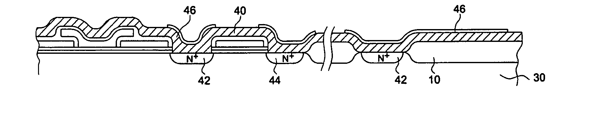
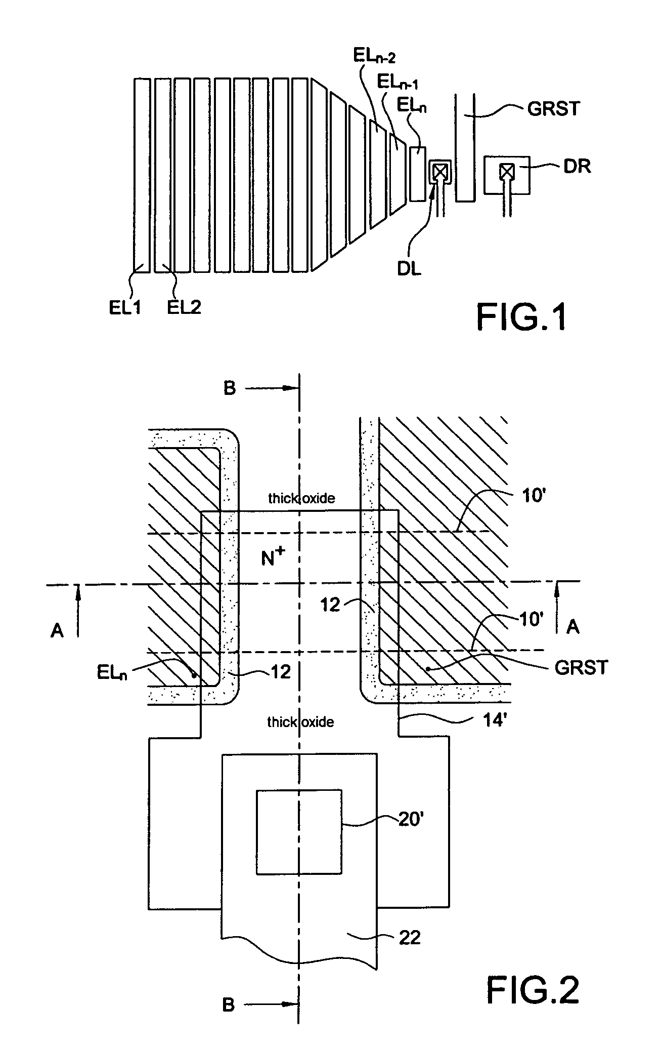
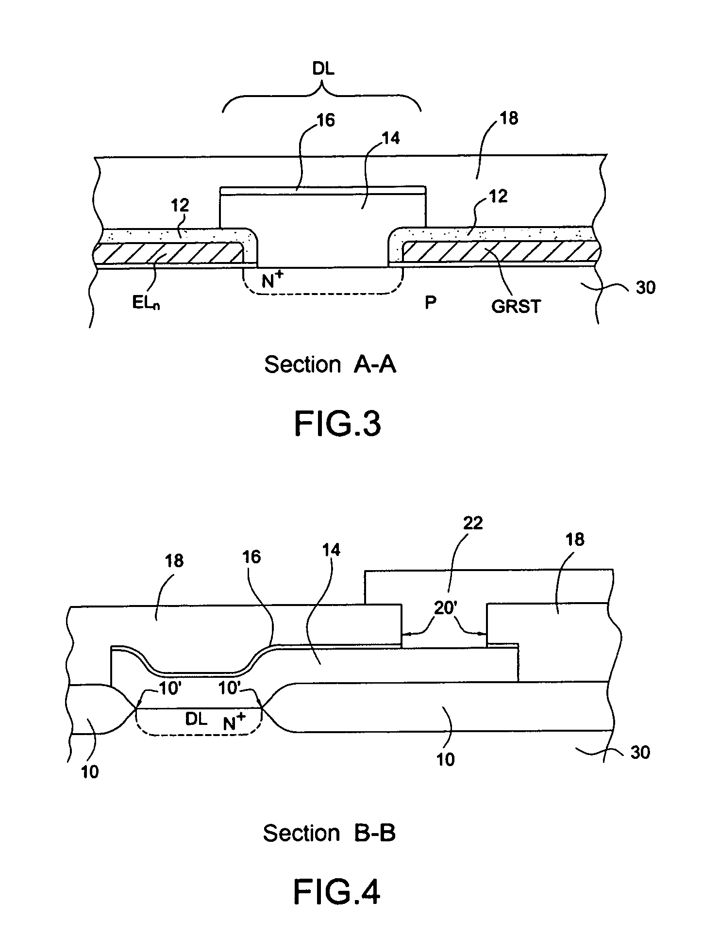
[0023] In FIG. 2 (plan view) and FIGS. 3 and 4 (sections along AA and B, respectively), the readout diode DL is defined by an N+-type doped zone diffused into the P-type substrate 30. The doped zone constitutes one pole of the diode, and the substrate constitutes another pole.

[0024] In the lateral direction of FIGS. 2 and 3 (on the left and on the right in FIG. 2 and in FIG. 3), this zone is delimited in practice by the edges of the two gates or electrodes ELn and GRST which frame it. The electrodes are hatched in FIGS. 2 and 3. In the vertical direction of the page in FIG. 2 (at the top and at the bottom in FIG. 2, on the left and on the right in FIG. 4), the N+-type diffused zone is delimited by thick oxide regions 10 (conventional LOCOS thermal oxide). The dashed lines 10′ of FIG. 2 represent the edges of the thick oxide zones 10 framing the diode. The zone corresponding to the diode DL does not comprise thick oxide.

[0025] The gates ELn and GRST are made of polycrystalline sili...


PUM


Abstract

The invention relates to integrated circuits comprising both conductive gates deposited above a semiconductor substrate and a diode is formed between two electrodes. In order to achieve a diode of very small dimensions, the following procedure is adopted: producing the electrodes (ELn, GRST, then thermally oxidizing the electrodes, then exposing the surface of the substrate between the electrodes, then the following operations: depositing doped polycrystalline silicon in order to form one pole (42) of the diode, the substrate forming the other pole, delimiting a desired silicon pattern covering the space left between the electrodes and also covering a region lying outside this space, depositing an insulating layer, locally etching an opening into this insulating layer above the polycrystalline silicon outside the space lying between the electrodes, in order to form an offset contact zone, depositing a metal layer and etching the metal layer.

Description

FIELD OF THE INVENTION [0001] The invention relates to integrated circuits comprising both conductive gates deposited above a semiconductor substrate and diodes formed in this substrate. BACKGROUND OF THE INVENTION [0002] The main application envisaged is a readout register for electrical charges, operating by charge transfer in the semiconductor substrate under the influence of variable potentials applied to gates juxtaposed above the substrate and insulated from the substrate. Such registers are present in matrix image sensors produced in CCD (charge coupled device) technology. They are used in particular to recover row-by-row the charges stored in a matrix of photosensitive elements in order to send them to a readout circuit, which converts them into electrical voltages or currents representing the level of charges photogenerated at each point of the row. [0003] The readout register consisting of juxtaposed gates or electrodes generally ends in a diode formed on the substrate, wh...

Claims


Application Information

Patent Timeline
IPC IPC(8): H01L21/44H01L29/768
CPCH01L29/76816H01L29/768
Inventor BLANCHARD, PIERRE
Owner ATMEL GRENOBLE
Why Eureka
Try Eureka