Strained silicon-on-insulator transistors with mesa isolation

a technology of straining silicon and isolation, applied in the field of straining silicon-on-insulator transistors formed with mesa isolation, can solve the problems of long time, high cost, and significant challenges

Inactive Publication Date: 2007-08-16
TAIWAN SEMICON MFG CO LTD
View PDF17 Cites 2 Cited by
  • Summary
  • Abstract
  • Description
  • Claims
  • Application Information

AI Technical Summary

Benefits of technology

[0006] Others have attempted to fabricate transistors on a strained silicon layer overlying two SiGe layers with different Ge contents which is provided on an insulator layer. In U.S. Pat. No. 6,410,371, a method of forming a semiconductor-on-insulator (SOI) wafer with a Si / SiGe / Si heterostructure is disclosed, where the topmost silicon layer is strained. These works teach the formation of SOI substrates comprising of Si and SiGe layers where the Si layer is strained. The presence of SiGe in the semiconductor layer introduces problems in the formation of liner oxide in the STI process. STI process also potentially relaxes the strained silicon layer.
[0009] It is therefore an object of the present invention to provide a silicon-on-insulator semiconductor device utilizing strained silicon technology.
[0013] In accordance with the present invention, a silicon-on-insulator semiconductor device and a method for fabricating the device are provided.
[0013] In accordance with the present invention, a silicon-on-insulator semiconductor device and a method for fabricating the device are provided.
[0011] It is a further object of the present invention to provide de a highly manufacturable strained silicon-on-insulator transistor with mesa isolation.

Problems solved by technology

Significant challenges are faced when CMOS devices are scaled into the sub-100 nm regime.
Such a thick graded buffer layer 12 requires an extended length of time, i.e., of several tens of minutes to several hours, to grow and is an expensive process.
However, such a substrate might not be easily or economically introduced into a conventional CMOS process.
The integration of strained layers into a conventional CMOS process introduce significant difficulties.
Since starting substrates with strained layers are subjected to the high thermal budget of the isolation formation process, the integration of strained layers on bulk substrates is very challenging.
In spite of this, U.S. Pat. No. 6,429,061 employs an expensive thick SiGe buffer layer and a selective strained silicon epitaxial process.
The presence of SiGe in the semiconductor layer introduces problems in the formation of liner oxide in the STI process.
This results in a liner oxide of poor quality and leads to leakage problems and poor device isolation.
However, the STI process still involves high temperatures that might relax the strained silicon layer.

Method used


Image

  • Strained silicon-on-insulator transistors with mesa isolation
  • Strained silicon-on-insulator transistors with mesa isolation
  • Strained silicon-on-insulator transistors with mesa isolation

Examples


Embodiment Construction

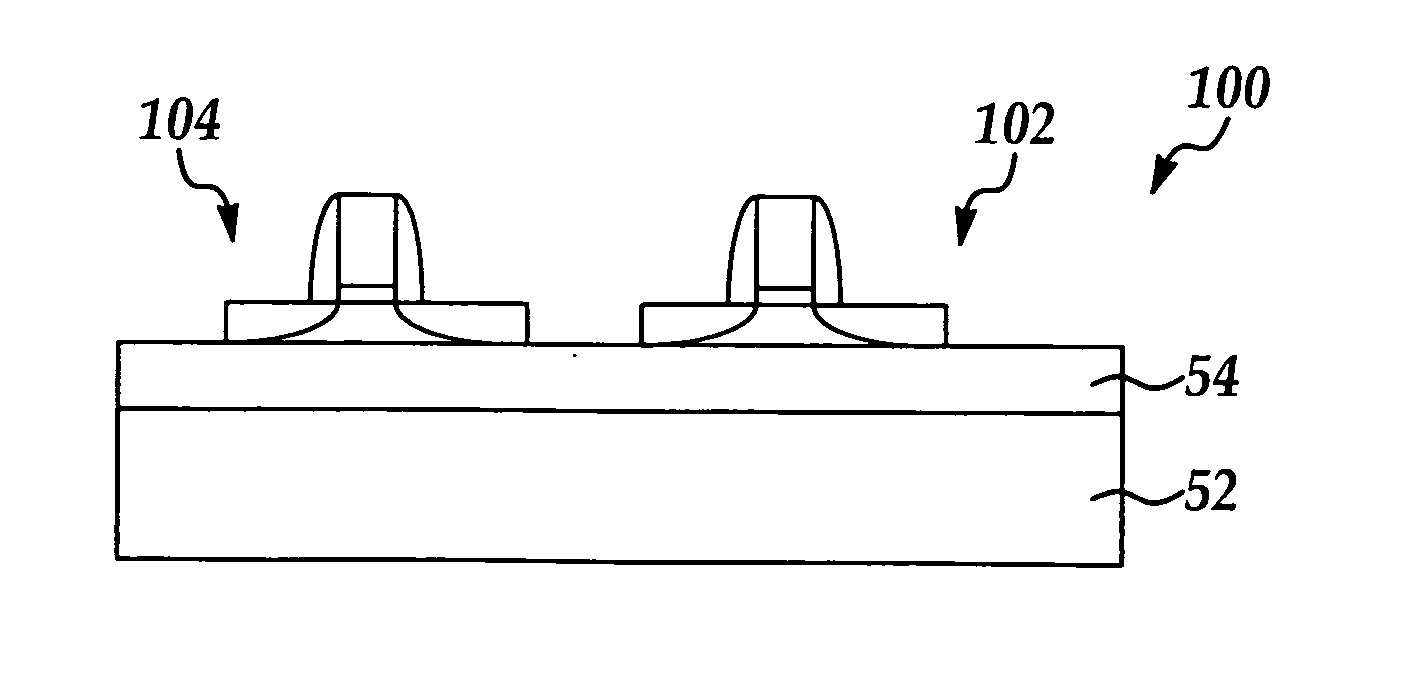
[0028] In the present invention, a strained silicon on insulator structure with mesa isolation is disclosed.

[0029] The present invention avoids the shortcomings of conventional devices and processes by disclosing a structure and a process where a strained silicon layer does not experience device isolation formation processes that require high temperatures, and where problems of liner oxide formation is eliminated. One isolation scheme without the use of high temperatures is mesa isolation. Mesa isolation relies on the formation of islands of active regions where device or transistors reside. The islands of active regions overlie an insulating substrate. Transistors residing on separate islands are therefore isolated from each other. The formation of islands of active regions does not involve high temperature steps. This is important for the retention of strain in the strained silicon layer. However, mesa isolation cannot be used in the conventional strained silicon substrate shown ...


PUM


Abstract

A silicon-on-insulator semiconductor device which includes a substrate; and insulator layer overlying the substrate; a plurality of strained silicon islands overlying the insulator layer, the strained silicon islands are isolated from each other by mesa isolation; and a plurality of transistors formed on the strained silicon islands. A method for fabricating the silicon-on-insulator semiconductor device is further disclosed.

Description

FIELD OF THE INVENTION [0001] The present invention generally relates to semiconductor devices and a method for making the same. More particularly, the invention is related to strained silicon-on-insulator transistors formed with mesa isolation. BACKGROUND OF THE INVENTION [0002] Complementary metal-oxide-semiconductor (CMOS) technology is the dominant semiconductor technology used for the manufacture of ultra-large scale integrated (ULSI) circuits today. Size reduction of the metal-oxide-semiconductor field-effect transistor (MOSFET) has provided significant improvement in the speed performance, circuit density, and cost per unit function of semiconductor chips over the past few decades. Significant challenges are faced when CMOS devices are scaled into the sub-100 nm regime. An attractive approach for additional improvement of CMOS transistor performance exploits strain-induced band-structure modification and mobility enhancement to increase the transistor drive current. Enhanced ...

Claims


Application Information

Patent Timeline
Patent Type & Authority Applications(United States)
IPC IPC(8): H01L21/84H01L21/762H01L27/12
CPCH01L21/76289H01L27/1203H01L21/84
Inventor YEO, YEE-CHIAHU, CHENMING
Owner TAIWAN SEMICON MFG CO LTD
Why Eureka
Try Eureka