Method for treating design errors of a layout of an integrated circuit

a technology of integrated circuits and layout errors, applied in computer aided design, program control, instruments, etc., can solve the problem of time-consuming and labor-intensive recording of waivers for each error that occurs

Inactive Publication Date: 2007-08-16
INFINEON TECH AG
View PDF8 Cites 25 Cited by
  • Summary
  • Abstract
  • Description
  • Claims
  • Application Information

AI Technical Summary

Problems solved by technology

An individual creation of the layout may result, in some cases, however, that errors detected with the aid of an automatic program in a comparison with the design rules are allowed, nevertheless.
In some cases, recording a waiver for each error that occurs may be time consuming, e.g., to the operator of a system.

Method used


Image

  • Method for treating design errors of a layout of an integrated circuit
  • Method for treating design errors of a layout of an integrated circuit
  • Method for treating design errors of a layout of an integrated circuit

Examples


Embodiment Construction

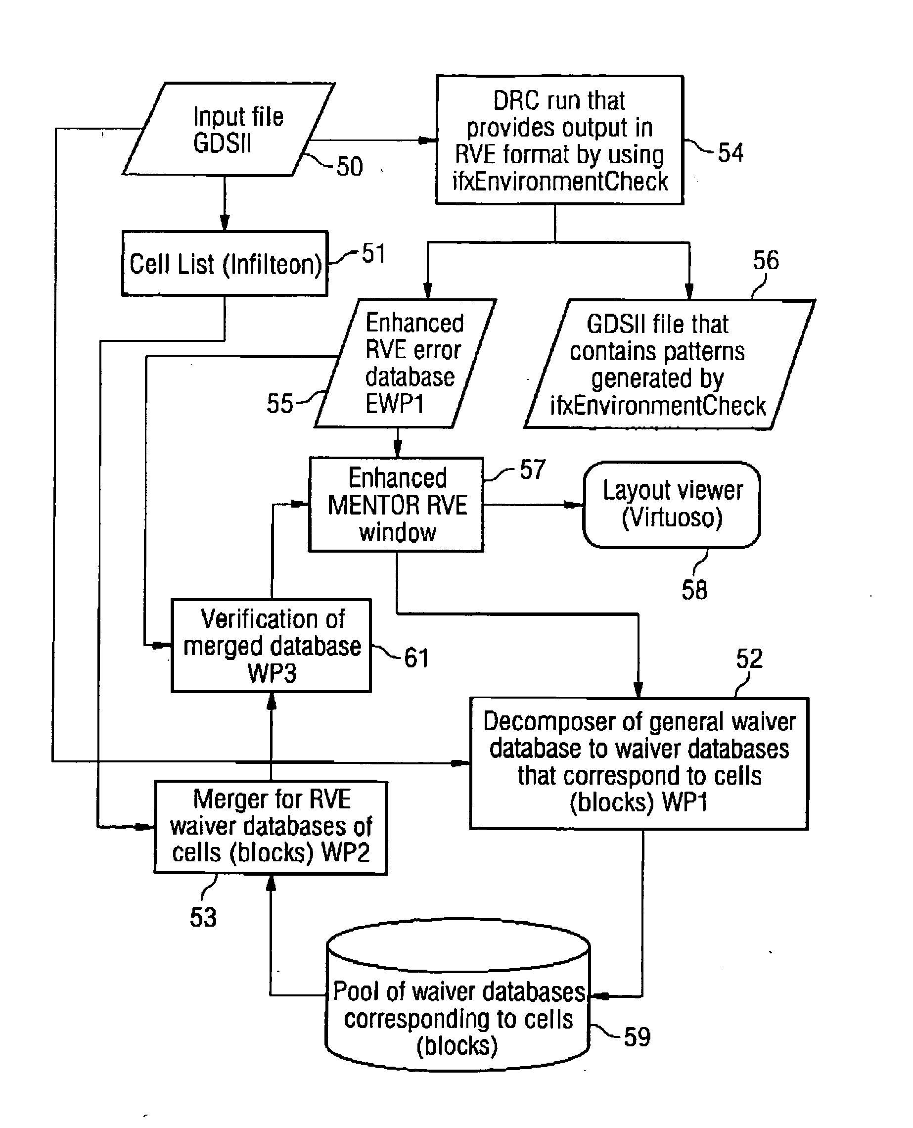
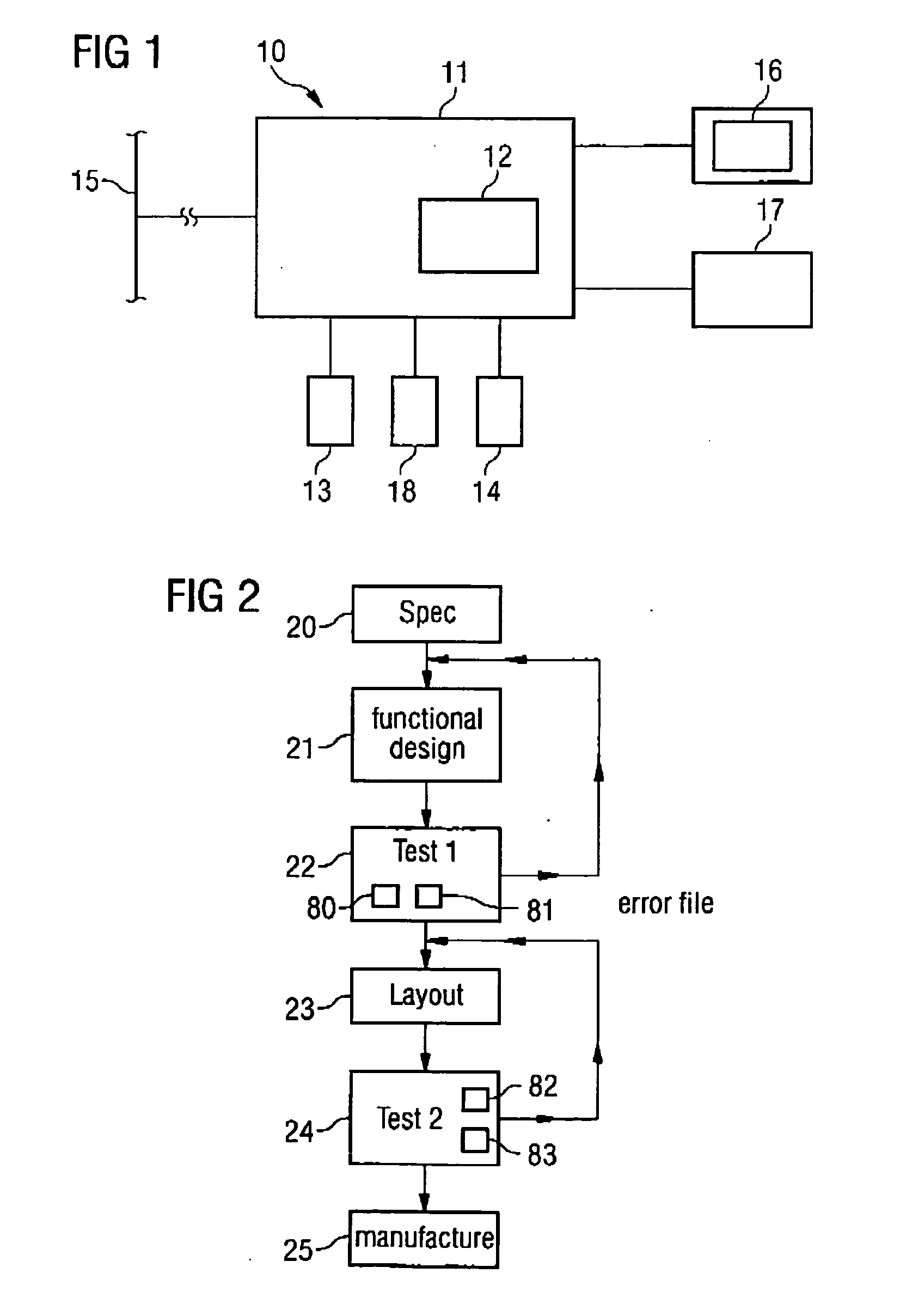
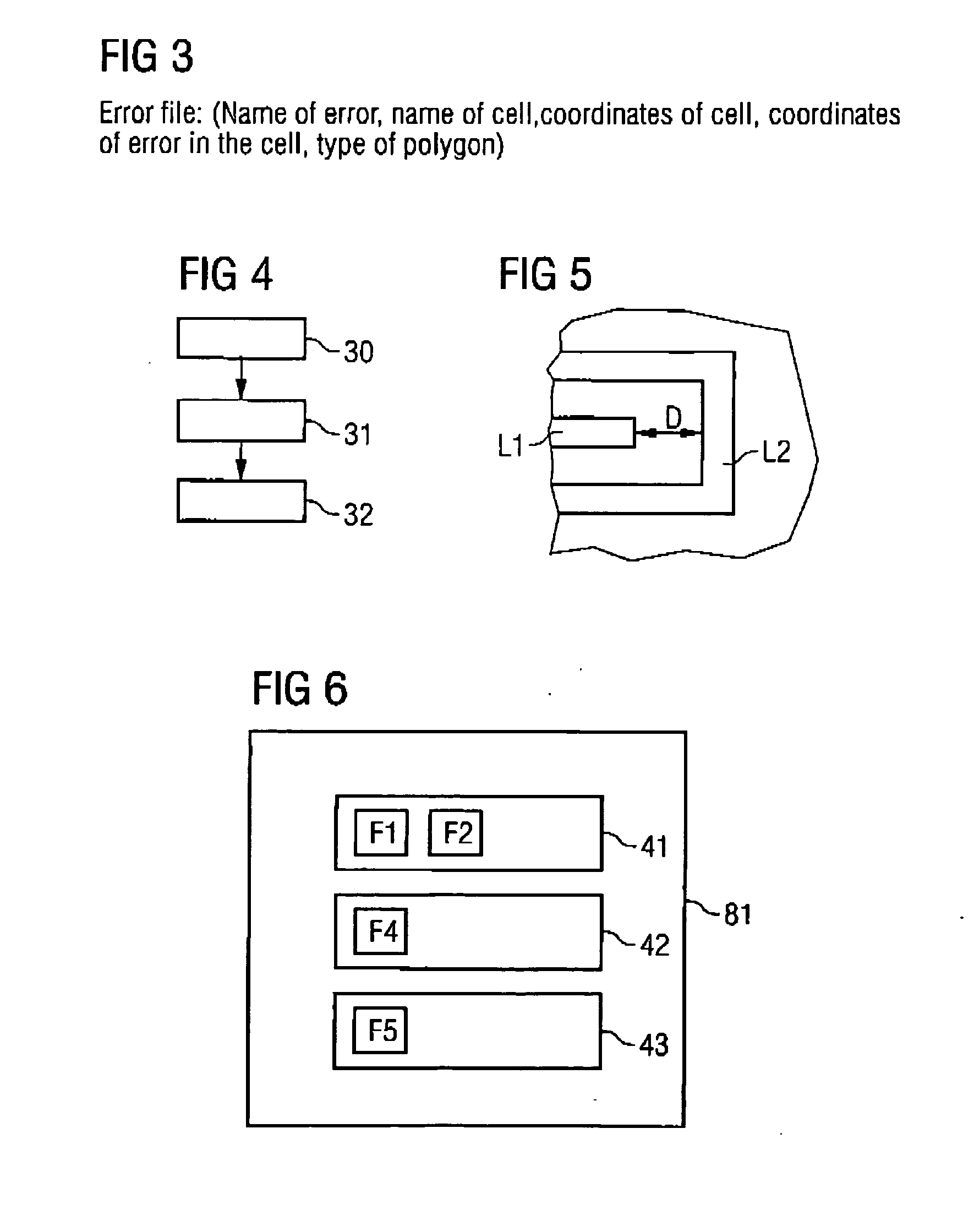
[0018] The invention relates to a method for treating design errors, wherein a design of an integrated circuit is checked by means of predetermined rules, wherein the design exhibits a number of cells, wherein an error is detected when the design deviates from the predetermined rules, wherein the error is written into an error file, wherein at least one detected error is written into a waiver file if the error is treated as an allowed error in spite of the deviation from the rules, wherein an allowed error is stored in the waiver file with specification of the cell in which the error occurs. Thus, in some cases, it may be possible to allocate allowed errors to a cell. Also, in some cases, it may be possible to provide increased flexibility in treating allowed errors.

[0019] In one embodiment, the method deals with layout errors, wherein a layout of an integrated circuit is checked by means of predetermined rules, wherein the layout exhibits a number of cells, wherein an error is det...


PUM


Abstract

Embodiments of the invention provide a method for treating errors during the checking of a design of an integrated circuit. In one embodiment, the method includes checking the design of the integrated circuit for errors using predetermined design rules, wherein the design includes a plurality of cells, detecting a design error when the design deviates from the predetermined design rules, writing the design error into a design error file, wherein at least one detected design error is written into a design waiver file if the design error is allowed as an allowed design error in spite of the deviation from the predetermined rules, and storing the allowed design error in the design waiver file with specification of a cell in which the design error occurs.

Description

BACKGROUND OF THE INVENTION [0001] 1. Field of the Invention [0002] The invention relates to a method for treating design errors of a layout of an integrated circuit. [0003] 2. Description of the Related Art [0004] The dimensions of integrated circuits are continuing to decrease so that parasitic effects play an ever greater role in the functionality of the integrated circuits. To avoid unwanted parasitic effects, during the development of integrated circuits it may be desired that the layout of the masks for producing the integrated circuits be accurately checked for errors. During the checking of the layout, a design rule check may be performed in order to check whether the patterns determined in the layout correspond to the predetermined rules. An individual creation of the layout may result, in some cases, however, that errors detected with the aid of an automatic program in a comparison with the design rules are allowed, nevertheless. This may make it possible to individually a...

Claims


Application Information

Patent Timeline
Patent Type & Authority Applications(United States)
IPC IPC(8): G06F17/50
CPCG06F17/5081G06F30/398
Inventor HOFSAESS, MARKUS
Owner INFINEON TECH AG
Why Eureka
Try Eureka