Masking process for simultaneously patterning separate regions

a masking process and patterning technology, applied in the direction of semiconductor devices, transistors, electrical equipment, etc., can solve the problems of increasing fabrication complexity, increasing fabrication time and expense,

Active Publication Date: 2007-09-06
MICRON TECH INC
View PDF99 Cites 80 Cited by
  • Summary
  • Abstract
  • Description
  • Claims
  • Application Information

AI Technical Summary

Problems solved by technology

While these improved transistor constructions are smaller and are packed more densely, they also often involve fabrication processes that are significantly more complex, therefore increasing fabrication time and expense.
Fabrication complexity is increased even further when high density vertical transistors are formed in an array on the same substrate as logic circuitry that is positioned adjacent to the transistor array.

Method used


Image

  • Masking process for simultaneously patterning separate regions
  • Masking process for simultaneously patterning separate regions
  • Masking process for simultaneously patterning separate regions

Examples


Embodiment Construction

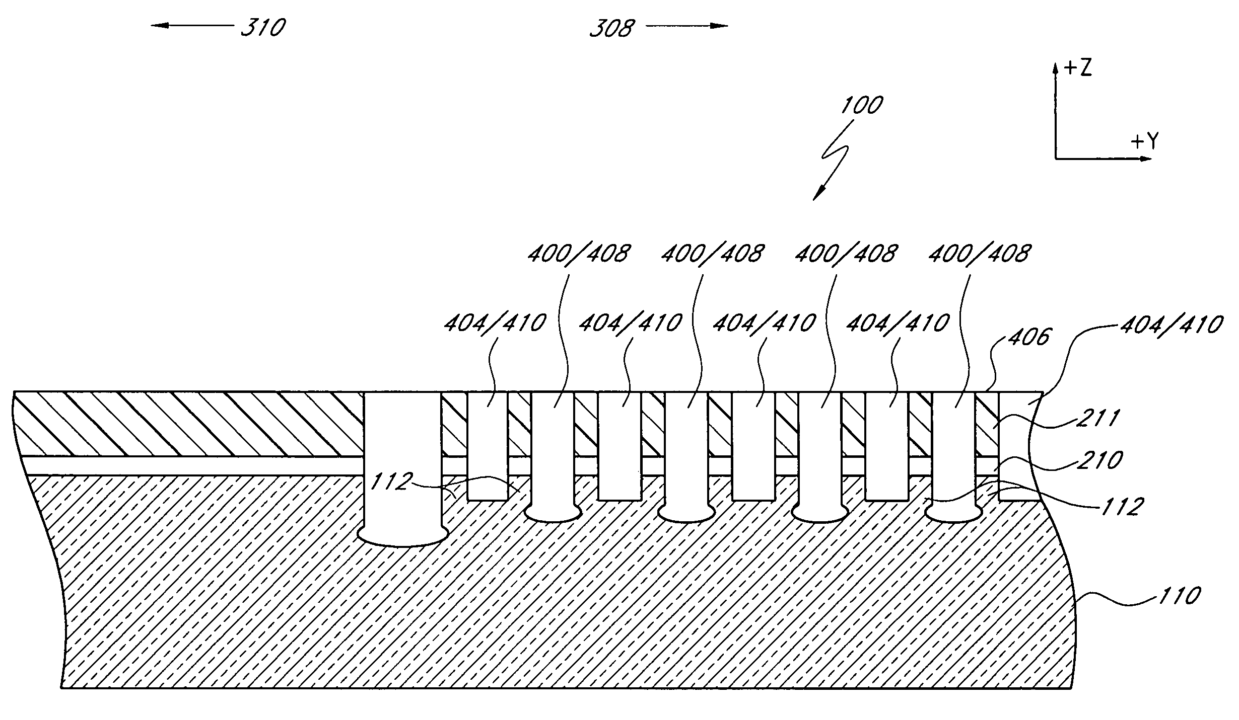
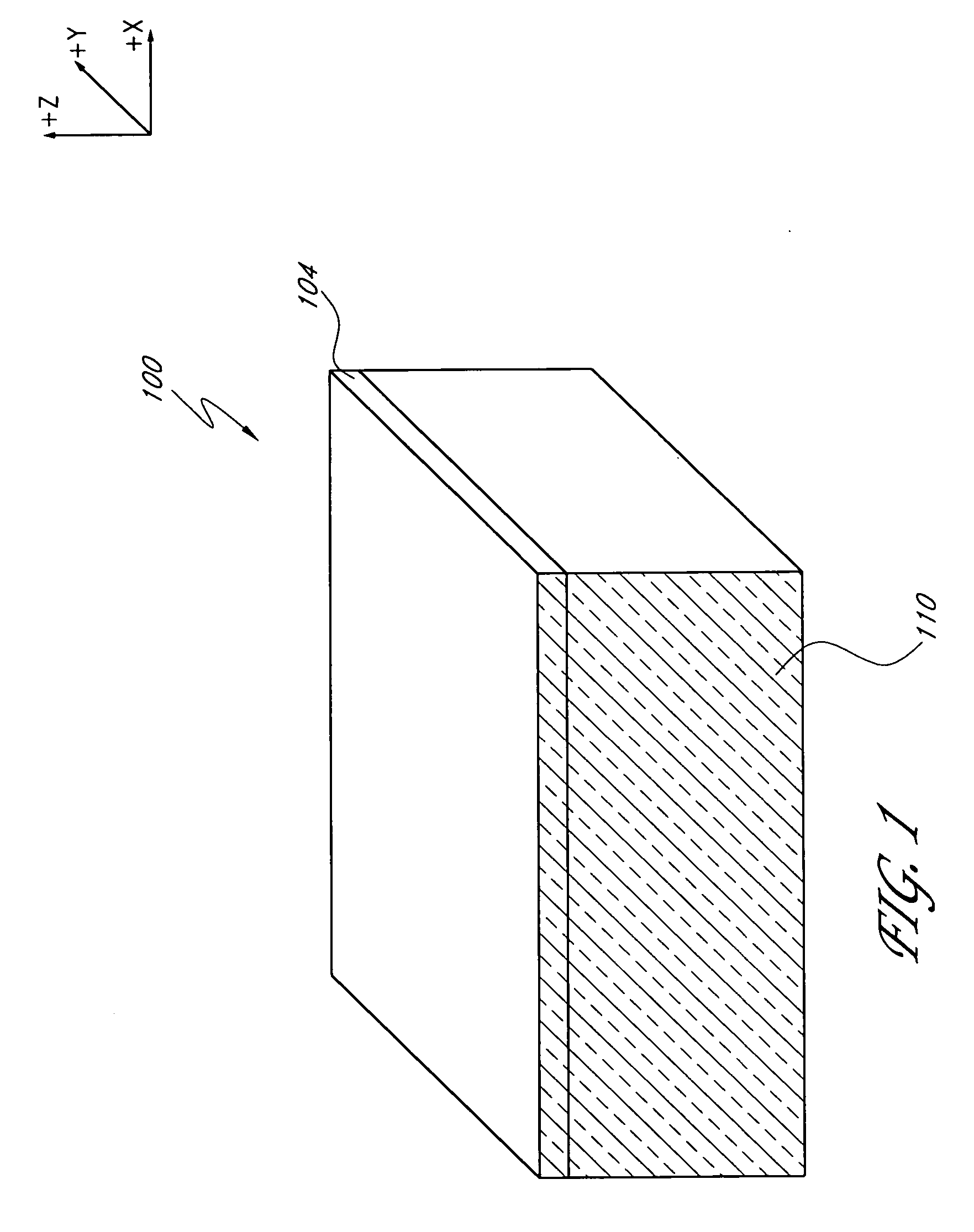
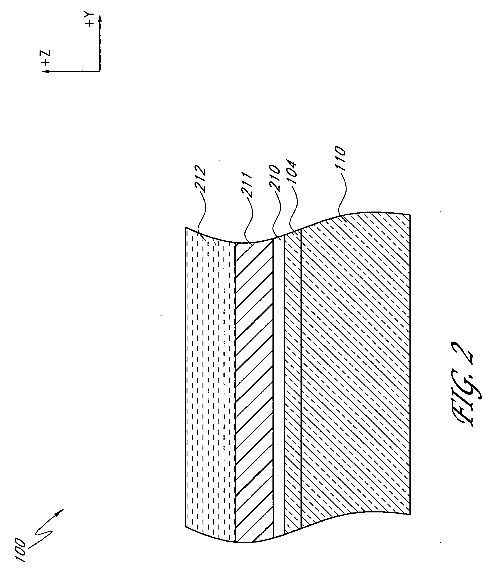
[0042] Disclosed herein are improved fabrication techniques for vertical transistor constructions. As disclosed above, vertical transistor constructions advantageously enable increased levels of device integration. The fabrication techniques disclosed herein advantageously use (a) fewer masking processes as compared to conventional fabrication techniques, and / or (b) masking processes that are easier to align. For example, certain of the embodiments disclosed herein advantageously enable the forming of active devices in the periphery region and patterning features (for example, intermediate trenches separating rows of transistors) in the array region with a single mask. Additionally, certain embodiments of the vertical transistors disclosed herein have a U-shaped configuration, wherein the channel connecting the source and drain regions is directly connected to the underlying substrate. This advantageously reduces or eliminates the floating body effect that is common in conventional ...


PUM


Abstract

According to another embodiment of the present invention, a method comprises patterning a first plurality of semiconductor structures in an array portion of a semiconductor substrate using a first photolithographic mask. The method further comprises patterning a second plurality of semiconductor structures over a logic portion of a semiconductor substrate using a second photolithographic mask. The method further comprises patterning a sacrificial layer over the first plurality of semiconductor structures using the second photolithographic mask. The sacrificial layer is patterned simultaneously with the second plurality of semiconductor structures.

Description

RELATED APPLICATIONS [0001] This application is related to U.S. patent application Ser. No. 10 / 933,062 (filed 1 Sep. 2004; Attorney Docket MICRON.299A; Micron Docket 2004-0398.00 / US), U.S. patent application Ser. No. 10 / 934,778 (filed 2 Sep. 2004; Attorney Docket MICRON.294A; Micron Docket 2003-1446.00 / US), U.S. patent application Ser. No. 10 / 855,429 (filed 26 May 2004; Attorney Docket MICRON.346A; Micron Docket 2003-1350.00 / US), U.S. patent application Ser. No. 11 / 201,824 (filed 10 Aug. 2005; Attorney Docket MICRON.346DV1; Micron Docket 2003-1350.01 / US), and U.S. patent application Ser. No. ______ (filed concurrently with this application; Attorney Docket MICRON.332A; Micron Docket 2005-0163.00 / US). The entire disclosure of each of these related applications is hereby incorporated by reference herein.FIELD OF THE INVENTION [0002] The present invention relates generally to methods for forming semiconductor structures, and relates more specifically to improved methods for forming ver...

Claims


Application Information

Patent Timeline
Patent Type & Authority Applications(United States)
IPC IPC(8): H01L29/768
CPCH01L21/0337H01L27/10876H01L27/108H01L27/088H01L27/10894H10B12/053H10B12/09H10B12/00
Inventor JUENGLING, WERNER
Owner MICRON TECH INC
Why Eureka
Try Eureka