Hybrid semiconductor device

Active Publication Date: 2007-09-13
INFINEON TECH AMERICAS
View PDF12 Cites 19 Cited by
  • Summary
  • Abstract
  • Description
  • Claims
  • Application Information

AI Technical Summary

Benefits of technology

[0007] It is an object of the present invention to provide a hybrid power device having a low po

Problems solved by technology

However, when conducting more than 5 A of current high voltage MOSFETS exhibit excessive power loss, and t

Method used


Image

  • Hybrid semiconductor device
  • Hybrid semiconductor device

Examples


Example

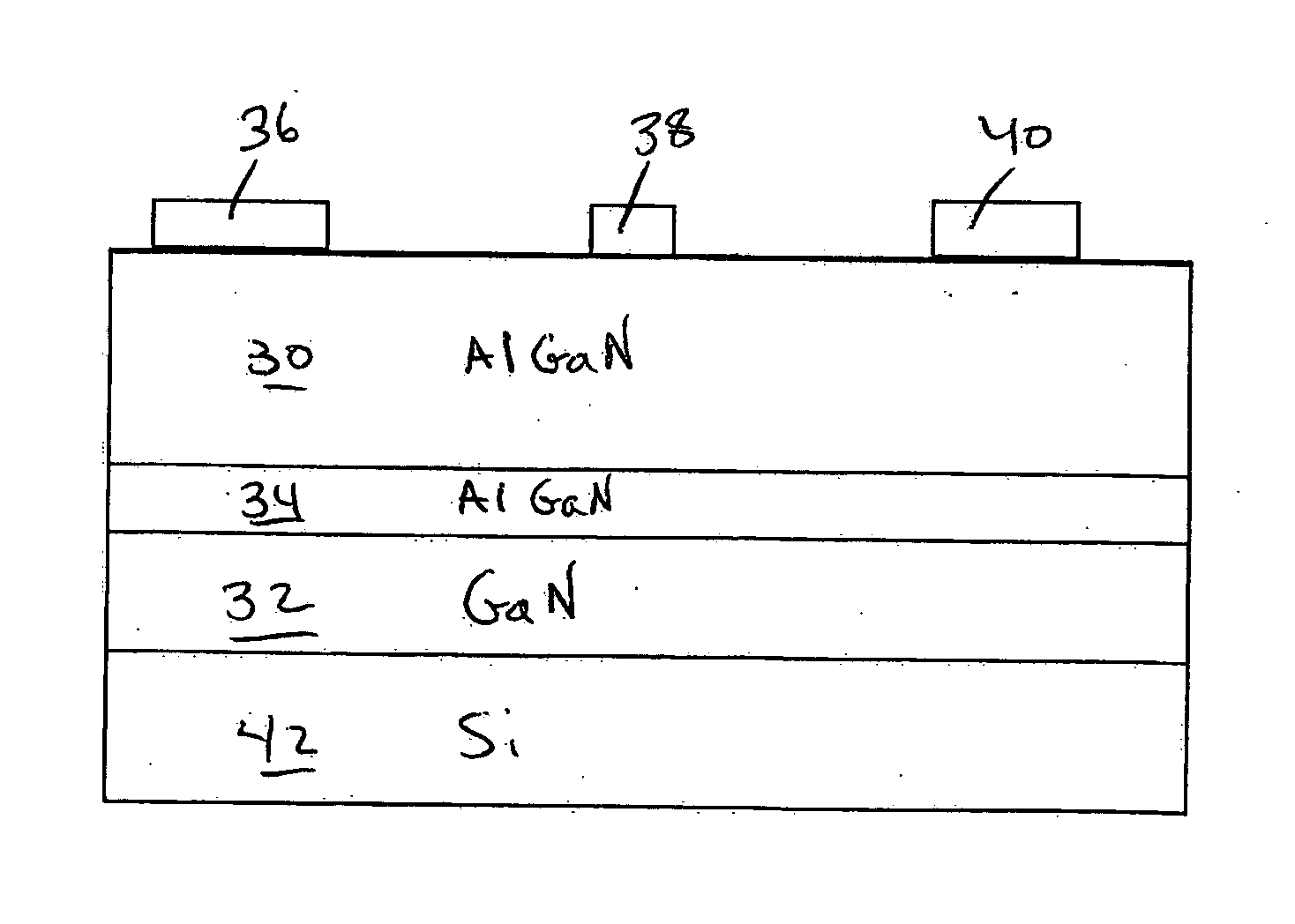
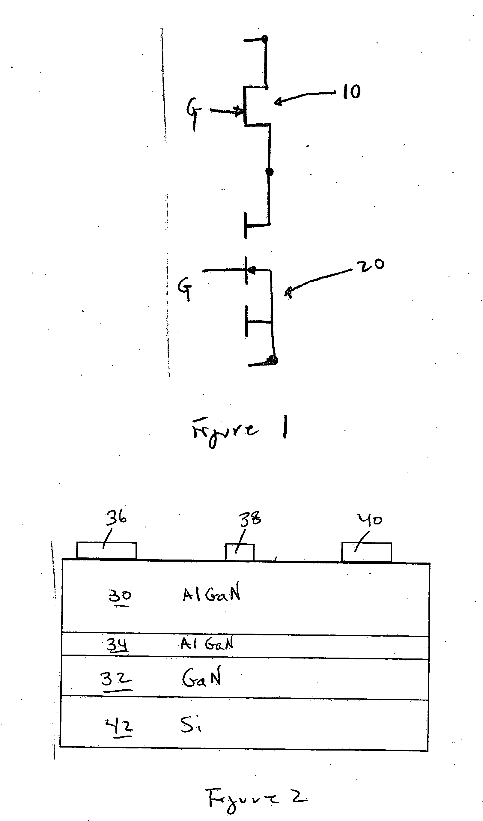
DETAILED DESCRIPTION OF THE DRAWINGS

[0016] Referring now to FIG. 1, a hybrid device according to the present invention includes a power semiconductor switching device, which may be silicon based power MOSFET 10, and GaN based device 20.

[0017] In a device according to the present invention, power MOSFET 10 is preferably connected with GaN based device 20 in a cascode configuration. That is, the drain electrode of power MOSFET 10 is connected with one of the electrodes of GaN based device 20 such that both devices will be in blocking mode under a reverse voltage condition. As a result, the capability of a device according to the present invention to withstand breakdown under reverse voltage conditions will be the combined capability of both devices. Thus, power MOSFET 10 and GaN based device 20 can be selected such that their combined breakdown voltage rating is equivalent to the breakdown voltage rating of a power semiconductor switching device of a higher rating. For example, a si...


PUM


Abstract

A hybrid device including a silicon based MOSFET operatively connected with a GaN based device.

Description

FIELD OF INVENTION [0001] The present invention relates power semiconductor device and more particularly to GaN based devices. BACKGROUND OF THE INVENTION [0002] Recent developments in electronic devices have created a demand for power devices that can supply higher currents. In addition to higher currents, it is important for power devices to operate more efficiently. [0003] One way of obtaining efficiency is to operate the power device at higher frequencies. Conventional silicon based high voltage power switching devices such as 600V MOSFETs exhibit desirable high frequency switching characteristics. However, when conducting more than 5 A of current high voltage MOSFETS exhibit excessive power loss, and thus poor efficiency. [0004] On the other hand low voltage power switching device can operate more efficiently at higher currents. The low breakdown voltage rating of low voltage power MOSFET is, however, a draw back. [0005] To take advantage of the efficiency of a low voltage powe...

Claims


Application Information

Patent Timeline
IPC IPC(8): H01L31/00
CPCH01L25/074H01L25/18H01L29/2003H01L29/7787H01L2924/0002H03K17/567H01L2924/00
Inventor LIDOW, ALEXANDERKINZER, DANIEL M.SRIDEVAN, SRIKANT
Owner INFINEON TECH AMERICAS
Why Eureka
Try Eureka