Driver circuit

Active Publication Date: 2014-02-27
FUJI ELECTRIC CO LTD
View PDF1 Cites 0 Cited by
  • Summary
  • Abstract
  • Description
  • Claims
  • Application Information

AI Technical Summary

Benefits of technology

[0025]According to the invention, as the period for which the high side detection transistor and low side detection transistor are simultaneously in an on-state is a short time at the end of the on-period of the high side detection transistor, and there is resistance in the current paths of the high side detection transistor and low side detection transistor, p

Problems solved by technology

In order to combat this, it is necessary to secure dead time longer than the longest of the varying delay times, as a result of which, high speed switching becomes difficult.
Also, as the circuit delay varies depending on the circuit configuration of the last stage of the dead time generator circuit and on operating conditions, a problem also occurs in that dead time setting is difficult.
When the level shifter circuit of Japanese Patent No. 3,384,399 (FIG. 5) is applied as it is to a driver circuit, the following kinds of problems occur.
A: As a large current contin

Method used


Image

  • Driver circuit
  • Driver circuit
  • Driver circuit

Examples


Example

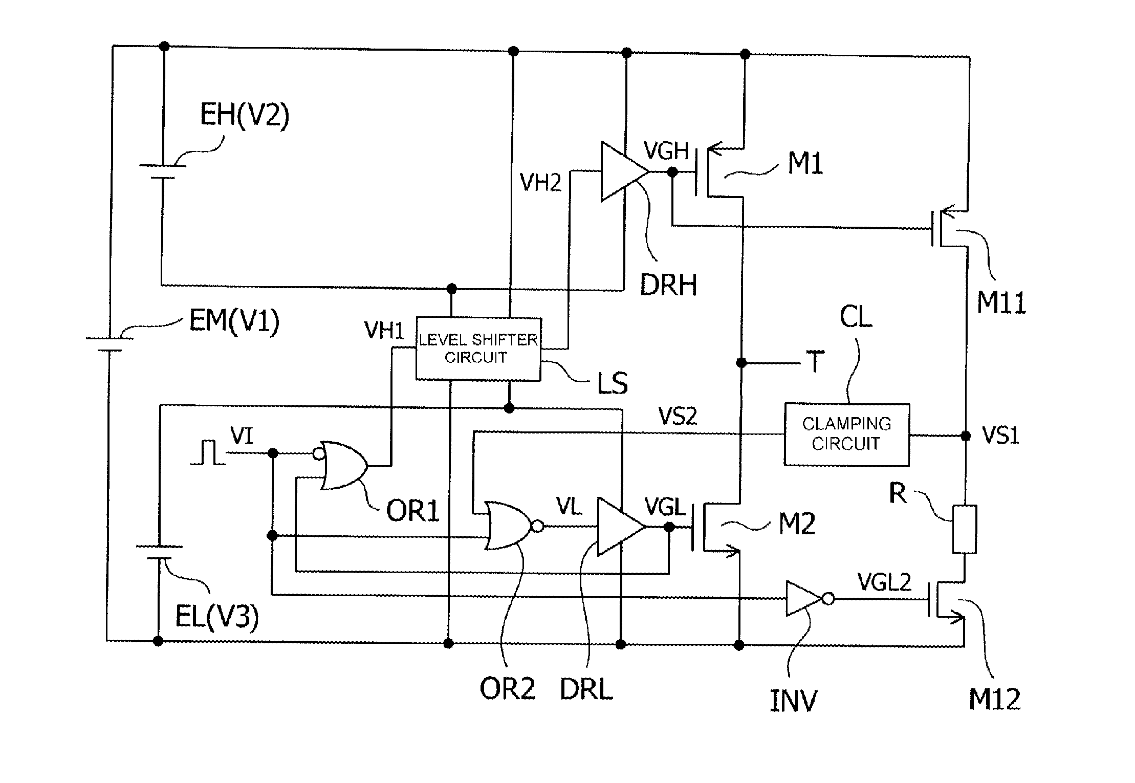
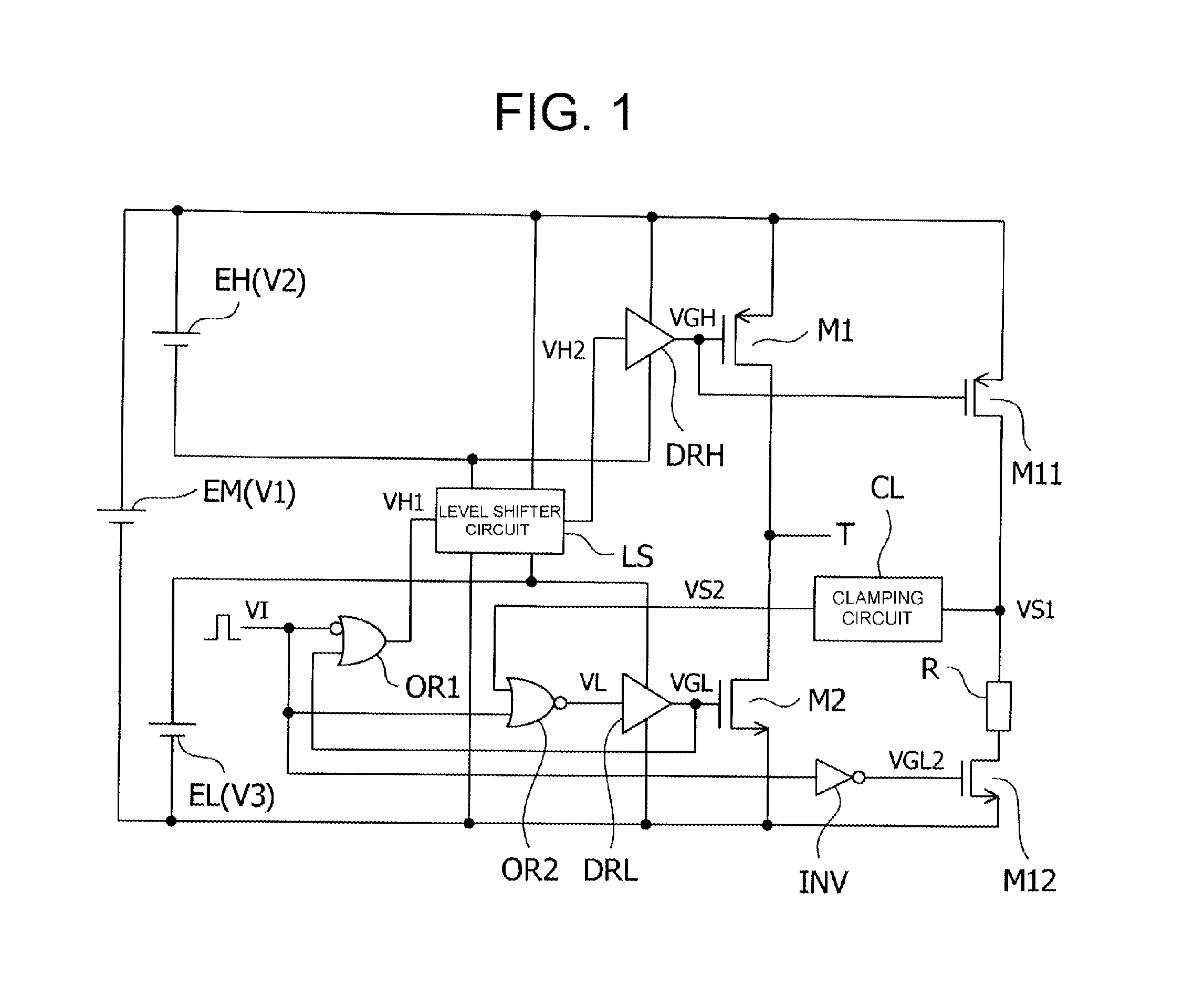
[0031]FIG. 1 shows one embodiment of a driver circuit according to the invention used for turning on and off a power semiconductor device (not shown).

[0032]The driver circuit includes a main power source EM, a high side power source EH, a low side power source EL, a high side output transistor M1, a high side first stage drive circuit DRH, a level shifter circuit LS, a low side output transistor M2, a low side first stage drive circuit DRL, a high side detection transistor M11 provided in order to detect a turning off of the high side output transistor M1, a low side detection transistor M12, also provided in order to detect a turning off of the high side output transistor M1, a resistor R, and a clamping circuit CL.

[0033]Normally, a p-channel metal oxide semiconductor field effect transistor (MOSFET) is used as the high side output transistor M1, while an n-channel MOSFET is used as the low side output transistor M2, as shown in the drawing.

[0034]Further, in the embodiment, a p-cha...


PUM


Abstract

A driver circuit has a detector circuit including a high side detection transistor, a resistor, and a low side detection transistor connected to a high side output transistor and a low side output transistor. A clamping circuit converts a high voltage amplitude change signal generated at a connection point of the high side detection transistor and resistor to a signal clamped to a voltage range applied on the low side. An OR circuit outputs a signal taking the logical sum of an inverted control signal and an output of a low side first stage drive circuit. A level shifter circuit outputs a level-shifted signal of the OR circuit to a high side first stage drive circuit. A second OR circuit outputs a signal wherein the logical sum of an output signal of the clamping circuit and the control signal is inverted to the low side first stage drive circuit.

Description

CROSS-REFERENCE TO RELATED APPLICATION[0001]This application claims priority under 35 U.S.C. §119 from Japanese Patent Application No. 2012-029447, filed on Feb. 14, 2012, the entirety of which is incorporated herein by reference.BACKGROUND OF THE INVENTION[0002]1. Technical Field[0003]The present invention relates to a driver circuit for turning a power semiconductor device on and off.[0004]2. Related Art[0005]A driver circuit is necessary in order to cause a turning on and off of a power semiconductor device. The driver circuit has a pulse signal as an input, and amplifies the input as far as power needed for turning the power semiconductor device on and off.[0006]One example of the driver circuit is shown in JP-A-2008-098920. The driver circuit of JP-A-2008-098920 includes an output buffer, formed of a high side output transistor (a p-channel field effect transistor) and a low side output transistor (an n-channel field effect transistor) that are turned on and off in a complement...

Claims


Application Information

Patent Timeline
IPC IPC(8): H03K17/04
CPCH03K17/04H03K17/04123
Inventor SUGAHARA, SATOSHI
Owner FUJI ELECTRIC CO LTD
Why Eureka
Try Eureka