
Element placement method and apparatus

a placement method and element technology, applied in the field of electronic circuit design, can solve the problems of chyan-breuer algorithm trapped in local minima, software algorithm and workstation capabilities not improving fast enough to keep up with the exponentially increasing number of resources available, and achieving the effects of improving quality, rapid prototyping, and substantial reduction in placement tim

Inactive Publication Date: 2007-09-13
CALIFORNIA INST OF TECH
View PDF31 Cites 29 Cited by
  • Summary
  • Abstract
  • Description
  • Claims
  • Application Information

AI Technical Summary

Benefits of technology

[0013] The present disclosure provides a spatial approach to the simulated annealing solution of the placement problem. According to the present disclosure, hardware can be constructed to mimic the structure of the problem, resulting in a solution to the placement problem that scales with the ability to build larger and larger devices.
[0023] Advantageously, stochastic swap considerations in accordance with the present invention improve quality, as shown in FIG. 4 and Chapter 6 of provisional application 60 / 473,722 incorporated by reference in the present application.
[0024] The present disclosure can be advantageously used in applications where the time criticality of the placement problem demands a fast solution, such as reconfigurable computing and logic emulation systems. In particular, physical devices for reconfigurable computing can be directly configured to be a placement engine, without adding additional hardware to the devices. In the case of logic emulation systems, arrays of FPGAs are usually adopted for rapid prototyping. According to the present disclosure, FPGAs can be used for self-placement, allowing a substantial reduction in the placement time when compared with software placement solutions.

Problems solved by technology

Software algorithms and workstation capabilities are not improving fast enough to keep up with the exponentially increasing number of resources available on FPGAs.
Placement is a NP-complete problem.
Force-directed algorithms can give acceptable results, but often terminate trapped in local minima.
Rarely, approaches to the placement problem are seen that involve a very large number of processing elements.
Unfortunately, this design mostly depends on a large-scale supercomputer.
However, also the Chyan-Breuer algorithm is trapped in local minima.
Prior art schemes are not able to achieve both high quality and large speedups.
Attempts to achieve high quality with simulated annealing either have limited quality or limited speedup.
None of the prior art schemes teaches how to employ large numbers of processors profitably to achieve large speedups, high quality, and avoid performance bottlenecks in communications.

Method used


Image

  • Element placement method and apparatus
  • Element placement method and apparatus
  • Element placement method and apparatus

Examples


first embodiment

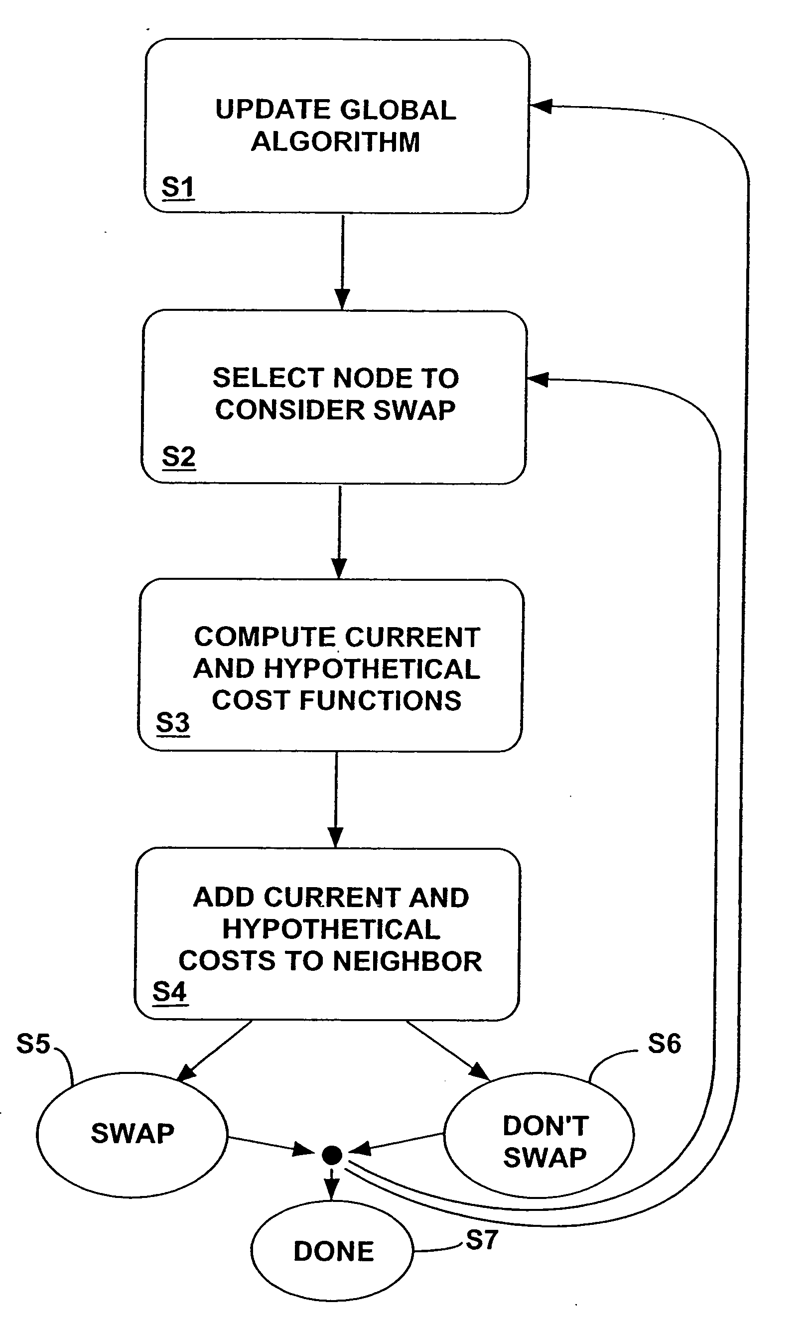
[0117] A first embodiment uses a “windowing” approach, as shown in FIG. 15, where placement has to be performed on a design of 20×20 elements, when only an array of 4×4 processing units is available. The windowing approach provides for movement of a window 300 across the design. In particular, a move could be either a horizontal move (arrows 301 or 302) or a vertical move (arrows 303 or 304). In particular, each time the nodes move, they stop considering the elements along one of their edges and add the elements along the opposing edge. The edge processing elements are responsible for communicating the updated information to a memory when the elements are removed from the window. The edge processing elements also bring in new information on elements which enter the region being processed.

second embodiment

[0118] A second embodiment uses a “folding” approach, where each processing unit is associated to more than one element. Once placement ends, the elements assigned to a particular processing unit can be arbitrarily assigned. Assuming, for example, that four elements are associated to each processing unit, the elements associated with the processing unit at (1, 1) can be assigned to (1, 1), (1, 2), (2, 1) and (2, 2), while the elements associated with the processing unit at (2, 2) can be assigned to (3, 3), (3, 4), (4, 3), and (4, 4) and so on.

[0119] Alternately, the processing unit can keep track of the multiple physical locations that it represents so that it does swap things into their final position. In addition to the external / neighbor swapping phases, an internal swapping phase can be added, in which the processing unit considers swaps among the cells that are associated with it. Also other optimization steps for the cells associated with it are possible.

[0120] The method desc...


PUM


Abstract

A method and a device for performing placement of a plurality of elements for circuit design. A potential location is assigned to each element and a placement engine is assigned to each potential location. Pairing operations are performed, in parallel, between placement engines to determine whether to perform exchange of the elements associated with the engines. Exchange determination is based both on a cost function and on randomness considerations. Also self-placement is allowed, where the placement engines are implemented on the same hardware system on which the elements are to be placed.

Description

CROSS REFERENCE TO RELATED APPLICATIONS [0001] This application is a divisional of U.S. application Ser. No. 10 / 643,772 filed on Aug. 18, 2003, which claims the benefit of U.S. provisional Patent Application Ser. No. 60 / 405,112 filed on Aug. 21, 2002 for a “Method and Apparatus for Hardware Acceleration of the Placement Problem” by Andre' DeHon and Michael Wrighton, U.S. provisional Patent Application Ser. No. 60 / 416,080 filed on Oct. 4, 2002 filed by Michael Wrighton and Andre' DeHon for “Hardware-assisted simulated annealing with application for fast FPGA Placement” and U.S. provisional Patent Application Ser. No. 60 / 473,722 filed on May 28, 2003 by Michael Wrighton for “Spatial Approach To FPGA Cell Placement By Simulated Annealing,” the disclosure of all of which is incorporated herein by reference.STATEMENT REGARDING FEDERALLY SPONSORED RESEARCH OR DEVELOPMENT [0002] The present invention was made with support from the United States Government under Grant number N00014-01-0651 ...

Claims


Application Information

Patent Timeline
Patent Type & Authority Applications(United States)
IPC IPC(8): G06F17/50
CPCG06F17/5072G06F30/392
Inventor DEHON, ANDREWRIGHTON, MICHAEL
Owner CALIFORNIA INST OF TECH
Learn More