Wide output swing CMOS imager

Inactive Publication Date: 2007-09-20
SHARP LAB OF AMERICA
View PDF4 Cites 23 Cited by
  • Summary
  • Abstract
  • Description
  • Claims
  • Application Information

AI Technical Summary

Benefits of technology

[0015] The present invention describes an APS imager cell made from a Si-on-insulator (SOI) substrate, using PMOS reset and source follower transistors. The use of PMOS transistors increases the output swing, without increasing supply voltage VDD. Since the pixel transistors are fabricated on the Si la

Problems solved by technology

Thus, the active pixel sensor of the prior art has poor performance under low power supply conditions.
However, as mentioned above in the description of FIG. 1, an NMOS transistor with VDD on both the gate and drain can only reach a source voltage of VDD−VT, thereby decreasing the dynamic range of the pixel.
The use of such a voltage is detrimental to device operation, however, as the higher voltage can damage the transistor.
This is especially true with advanced IC technologies that use a very thin ga

Method used


Image

  • Wide output swing CMOS imager
  • Wide output swing CMOS imager
  • Wide output swing CMOS imager

Examples


Embodiment Construction

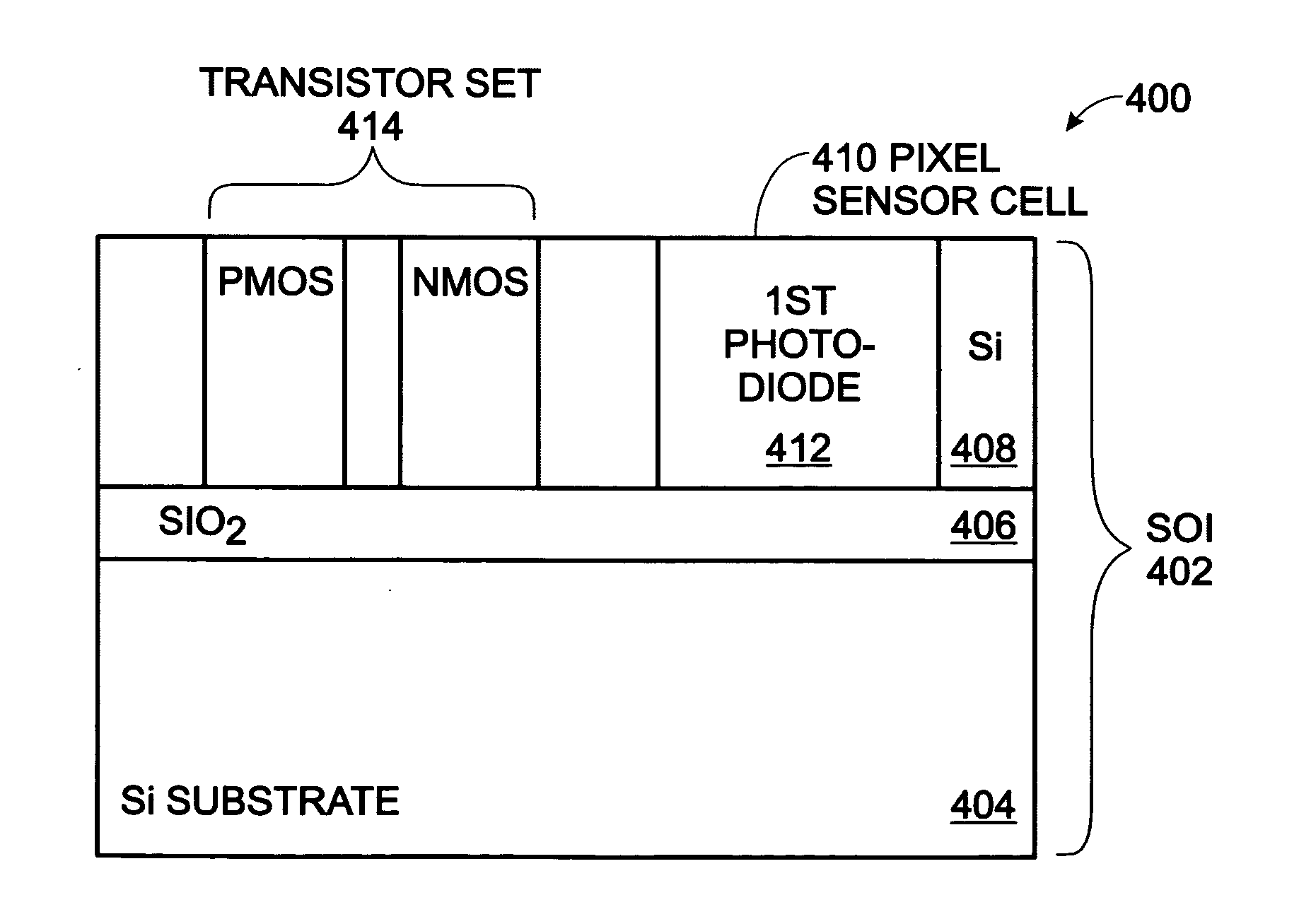
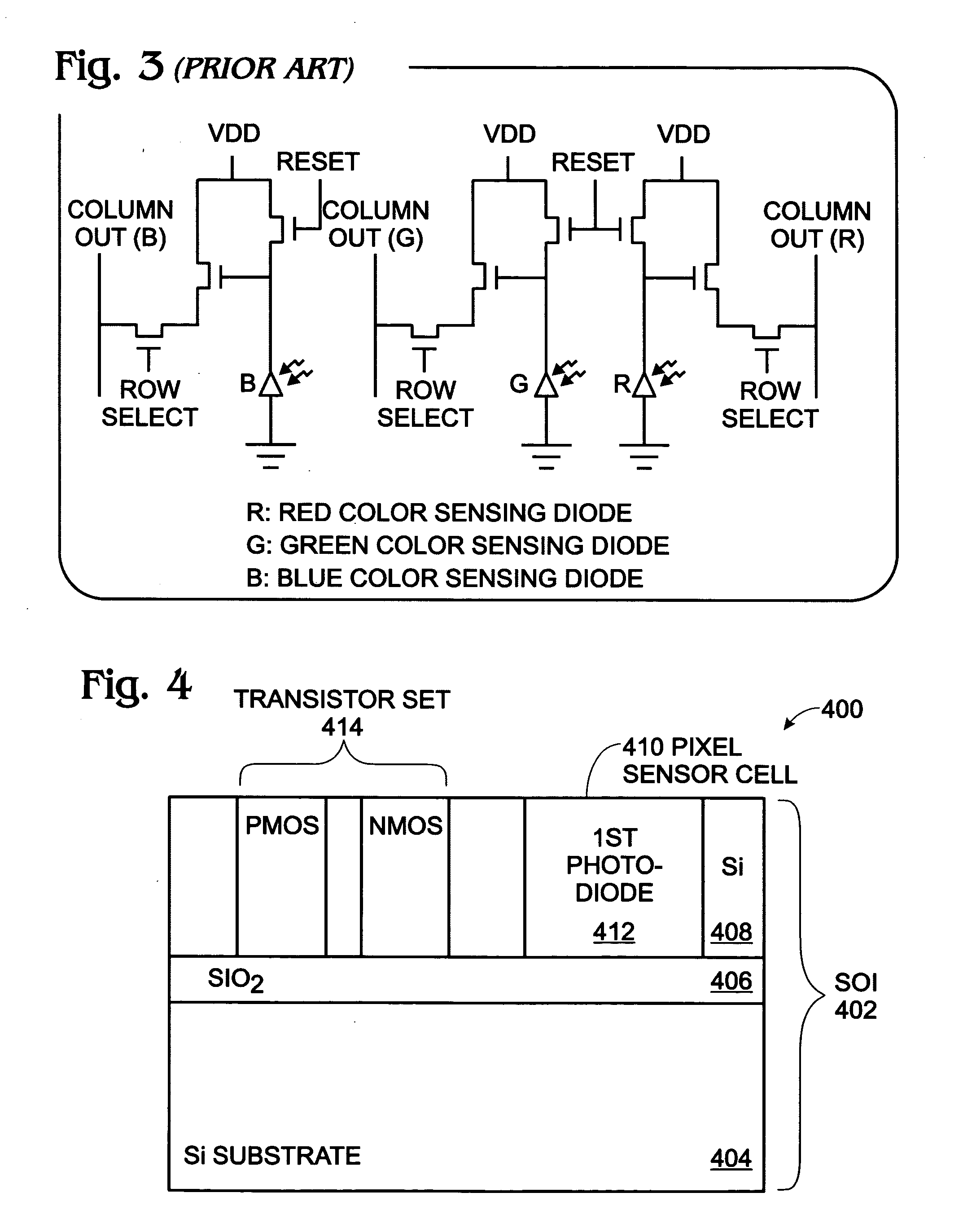
[0030]FIG. 4 is a schematic block diagram depicting a CMOS APS imager cell on a silicon-on-insulator (SOI) substrate. The APS imager cell is comprised of a pixel sensor cell and a pixel transistor set. The APS imager cell 400 comprises a SOI substrate 402 including a silicon (Si) substrate 404, a silicon dioxide insulator 406 overlying the substrate 404, and a Si top layer 408 overlying the insulator 406. A pixel sensor cell 410, including a photodiode 412, is formed in the Si top layer 408 of the SOI substrate 402. A pixel transistor set 414 is also formed in the SOI top Si layer 408 and connected to the pixel sensor cell 410. As described in more detail below, the pixel transistor set 414 includes at least one p-channel MOS (PMOS) transistor and at least one n-channel MOS (NMOS) transistor. Typically, the pixel transistor set 414 is a three-transistor (3T) set for use with a single photodiode, or a nine-transistor (9T) or a six-transistor (6T) cell, for use with stacked (multiple)...


PUM


Abstract

A CMOS active pixel sensor (APS) imager cell is provided on a silicon-on-insulator (SOI) substrate. The APS imager cell is made from a SOI substrate including a silicon (Si) substrate, a silicon dioxide insulator overlying the substrate, and a Si top layer overlying the insulator. A pixel sensor cell including a photodiode is formed in the Si top layer of the SOI substrate. A pixel transistor set is formed in the SOI top Si layer and connected to the pixel sensor cell. The pixel transistor set includes at least one p-channel MOS (PMOS) transistor and at least one n-channel MOS (NMOS) transistor. In the case of a three-transistor (3T) pixel transistor set, the selected transistor is NMOS, the reset transistor is PMOS, and the source follower may be either NMOS or PMOS.

Description

RELATED APPLICATIONS [0001] This application is a Continuation-in-Part of a pending patent application entitled, A REAL-TIME CMOS IMAGER HAVING STACKED PHOTODIODES FABRICATED ON SOI WAFER, invented by Lee et al., Ser. No. 11 / 384,110, filed Mar. 17, 2006, Attorney Docket No. SLA8033, which is incorporated herein by reference.BACKGROUND OF THE INVENTION [0002] 1. Field of the Invention [0003] This invention generally relates complementary metal / oxide / semiconductor (CMOS) imaging sensors and, more particularly, to an imager pixel sensor cell made from a combination of n-channel MOS devices, p-channel MOS devices, and photodiodes on a silicon-on-insulator (SOI) substrate. [0004] 2. Description of the Related Art [0005]FIG. 1 is a schematic diagram depicting an active pixel sensor (APS) imager cell made with n-channel MOS (NMOS) transistors (prior art). The APS cell includes a reset transistor, source follower transistor, select transistor, and a photodiode. All three transistors in the ...

Claims


Application Information

Patent Timeline
IPC IPC(8): H01L21/00
CPCH01L27/14603H01L27/14632H01L27/14689H01L27/14647H01L27/14683H01L27/14645
Inventor LEE, JONG-JANHSU, SHENG TENG
Owner SHARP LAB OF AMERICA
Why Eureka
Try Eureka