High efficiency and/or high power density wide bandgap transistors

a transistor and wide bandgap technology, applied in the field of wide bandgap transistors, can solve the problems of low cutoff frequency, fabricated devices, and less familiar semiconductor materials that are not well suited for higher power and/or high frequency applications, and achieve the effect of modulating the conductivity of the channel layer

Active Publication Date: 2007-10-11
WOLFSPEED INC
View PDF35 Cites 95 Cited by
  • Summary
  • Abstract
  • Description
  • Claims
  • Application Information

AI Technical Summary

Benefits of technology

[0011] A field effect transistor according to some embodiments of the invention includes a Group III-nitride channel layer, and a gate contact on the Group III-nitride channel layer and configured to modulate a conductivity of the channel layer when a voltage is applied to the gate contact. The gate contact may have a length configured to permit modulation of the conductivity of the channel layer at frequencies exceeding 1 GHz. Source and drain contacts are on the Group III-nitride channel layer, an insulating layer is on the gate contact, and a field plate is on the insulating layer and is electrically coupled to the source contact. The field effect transistor may exhibit a power density of greater than 40 W / mm under continuous wave or pulsed operation at a frequency of at least 4 GHz.

Problems solved by technology

These more familiar semiconductor materials may not be well suited for higher power and / or high frequency applications, however, because of their relatively small bandgaps (e.g., 1.12 eV for Si and 1.42 for GaAs at room temperature) and / or relatively small breakdown voltages.
However, fabricated devices at that time had low cutoff frequencies, and were not suitable for microwave operation.
However, such a configuration may impose large parasitic capacitances.

Method used


Image

  • High efficiency and/or high power density wide bandgap transistors
  • High efficiency and/or high power density wide bandgap transistors
  • High efficiency and/or high power density wide bandgap transistors

Examples


example devices

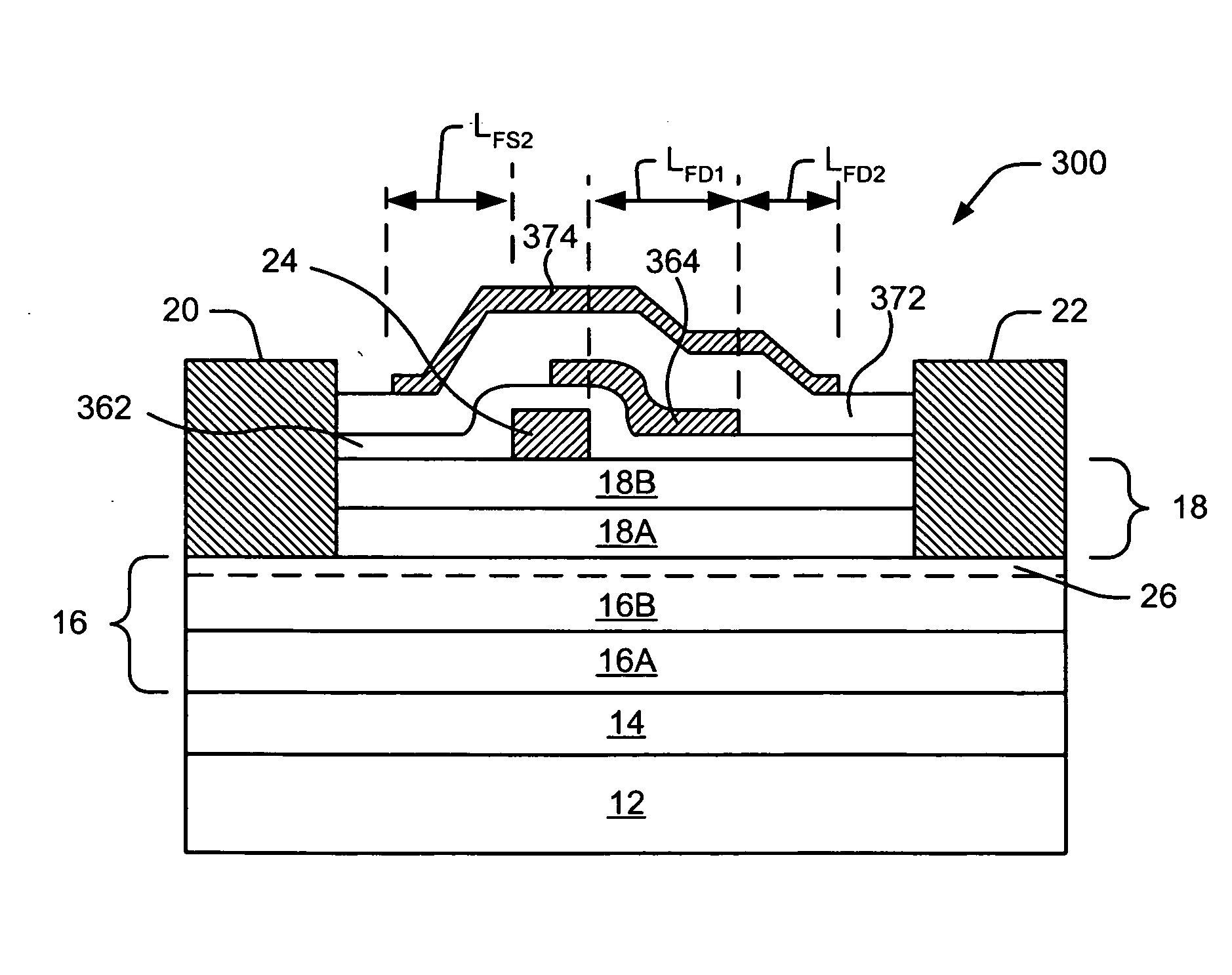
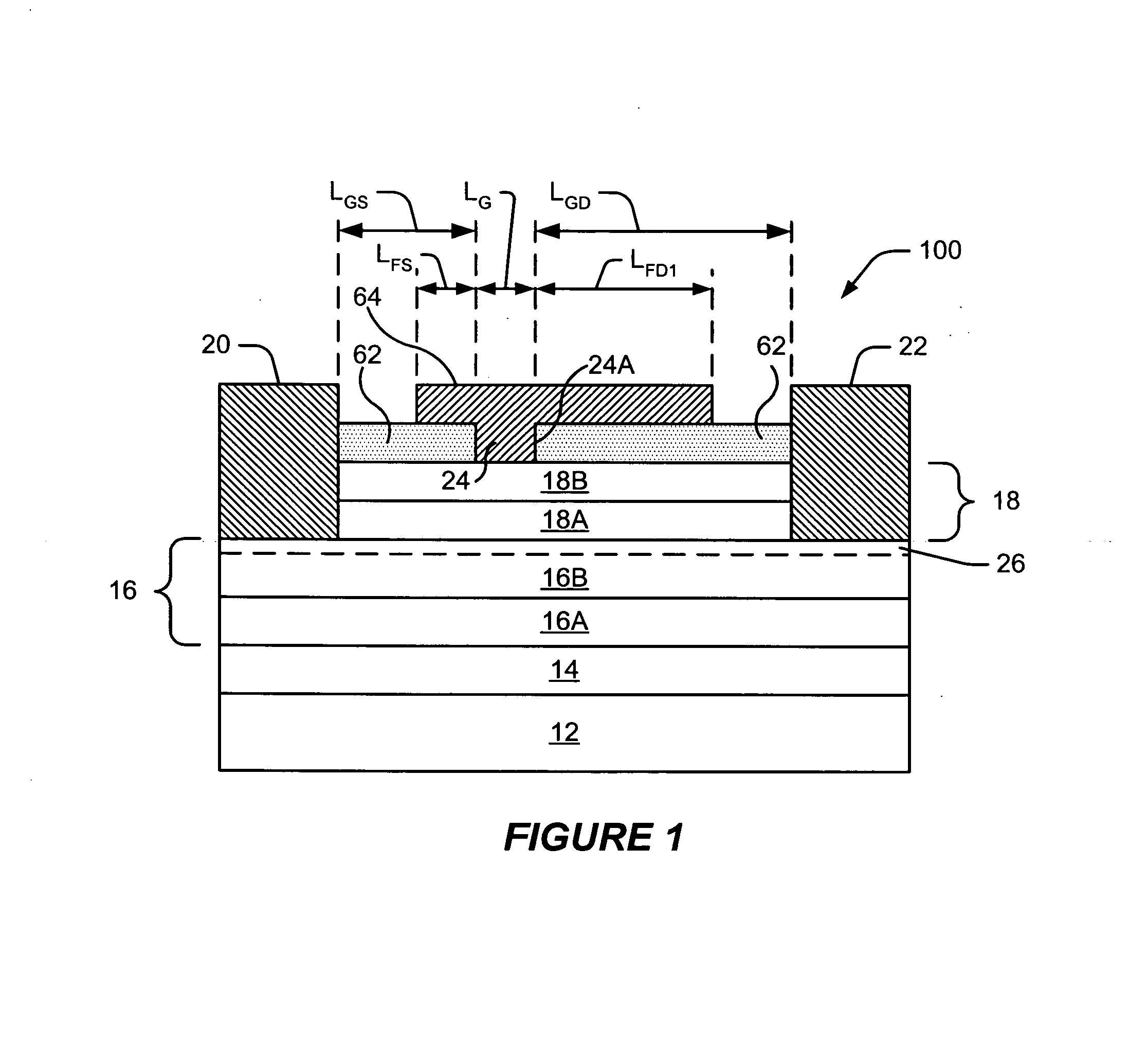
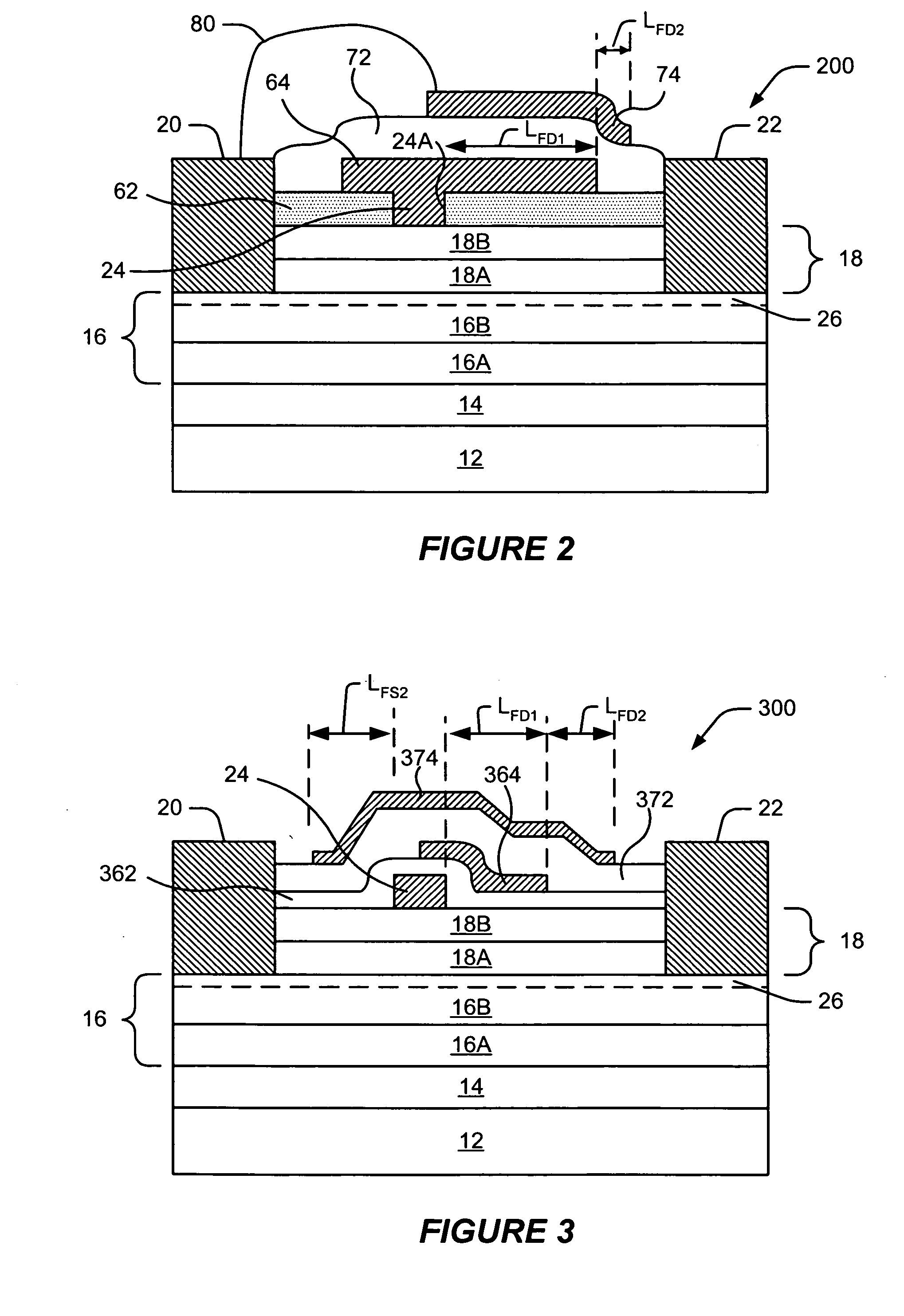
[0096] A first exemplary device having a single field plate structure includes a high purity semi-insulating SiC substrate 12. An AIN buffer layer 14 is formed on the substrate 12 and has a thickness of about 200 nm. A GaN first channel sublayer 16A is provided on the buffer layer 12 and has a thickness of about 0.8 μm. The first channel sublayer 16A is doped with Fe at a concentration of about 1×10¹⁸ / cm3. A GaN second channel sublayer 16B having a thickness of about 0.8 μm is formed on the first channel sublayer 1-6A. The second channel sublayer 16B is unintentionally doped, but has a residual concentration of Fe dopants therein that decreases with distance from the first channel sublayer 16A.

[0097] A first barrier sublayer 18A is provided on the second channel sublayer 16B. The first barrier layer is formed of AIN and has a thickness of about 0.8 nm. A second barrier layer 18B, including AlGaN with about 25% Al, is provided on the first barrier sublayer 18A and has a thickness of...


PUM


Abstract

Field effect transistors having a power density of greater than 40 W/mm when operated at a frequency of at least 4 GHz are provided. The power density of at least 40 W/mm may be provided at a drain voltage of 135 V. Transistors with greater than 60% PAE and a power density of at least 5 W/mm when operated at 10 GHz at drain biases from 28 V to 48 V are also provided.

Description

FIELD OF THE INVENTION [0001] The present invention relates to semiconductor devices and, more particularly, to wide bandgap transistors. BACKGROUND [0002] Materials such as silicon (Si) and gallium arsenide (GaAs) have found wide application in semiconductor devices. These more familiar semiconductor materials may not be well suited for higher power and / or high frequency applications, however, because of their relatively small bandgaps (e.g., 1.12 eV for Si and 1.42 for GaAs at room temperature) and / or relatively small breakdown voltages. [0003] Accordingly, interest in high power, high temperature and / or high frequency applications and devices has turned to wide bandgap semiconductor materials such as silicon carbide (2.996 eV for alpha SiC at room temperature) and the Group III nitrides (e.g., 3.36 eV for GaN at room temperature). These materials typically have higher electric field breakdown strengths and higher electron saturation velocities as compared to gallium arsenide and ...

Claims


Application Information

Patent Timeline
Patent Type & Authority Applications(United States)
IPC IPC(8): H01L29/76
CPCH01L29/2003H01L29/7787H01L29/42316H01L29/402H01L29/404H01L29/66462
Inventor WU, YIFENGPARIKH, PRIMITMISHRA, UMESHMOORE, MARCIA
Owner WOLFSPEED INC
Why Eureka
Try Eureka