

Infrared interferometric-spatial-phase imaging using backside wafer marks
a technology of infrared interferometry and spatial phase, applied in the field of angstrom-level alignment and position, can solve the problem of insufficient application for many applications
- Summary
- Abstract
- Description
- Claims
- Application Information
AI Technical Summary
Benefits of technology
Problems solved by technology
Method used
Image

Examples
Embodiment Construction
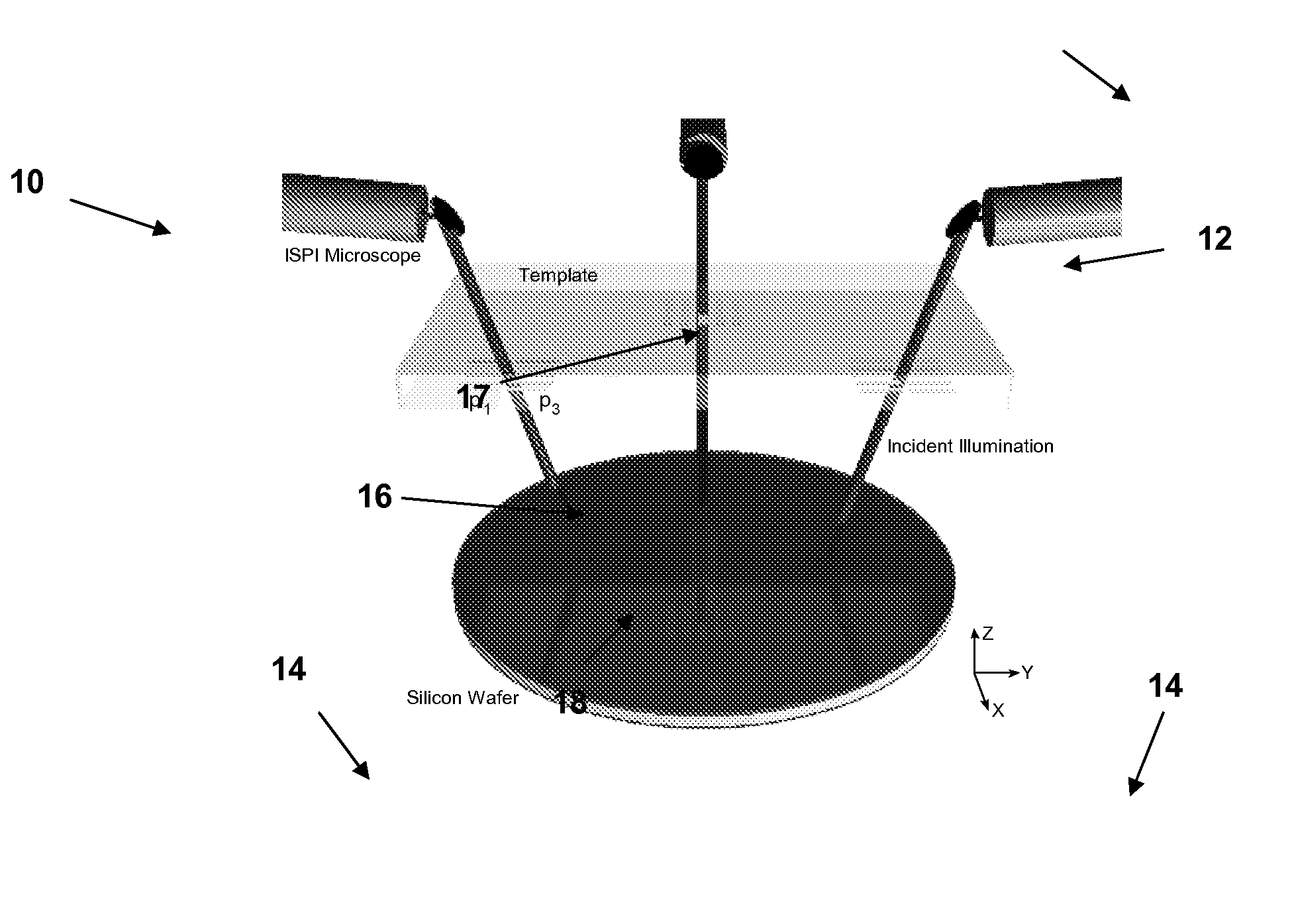
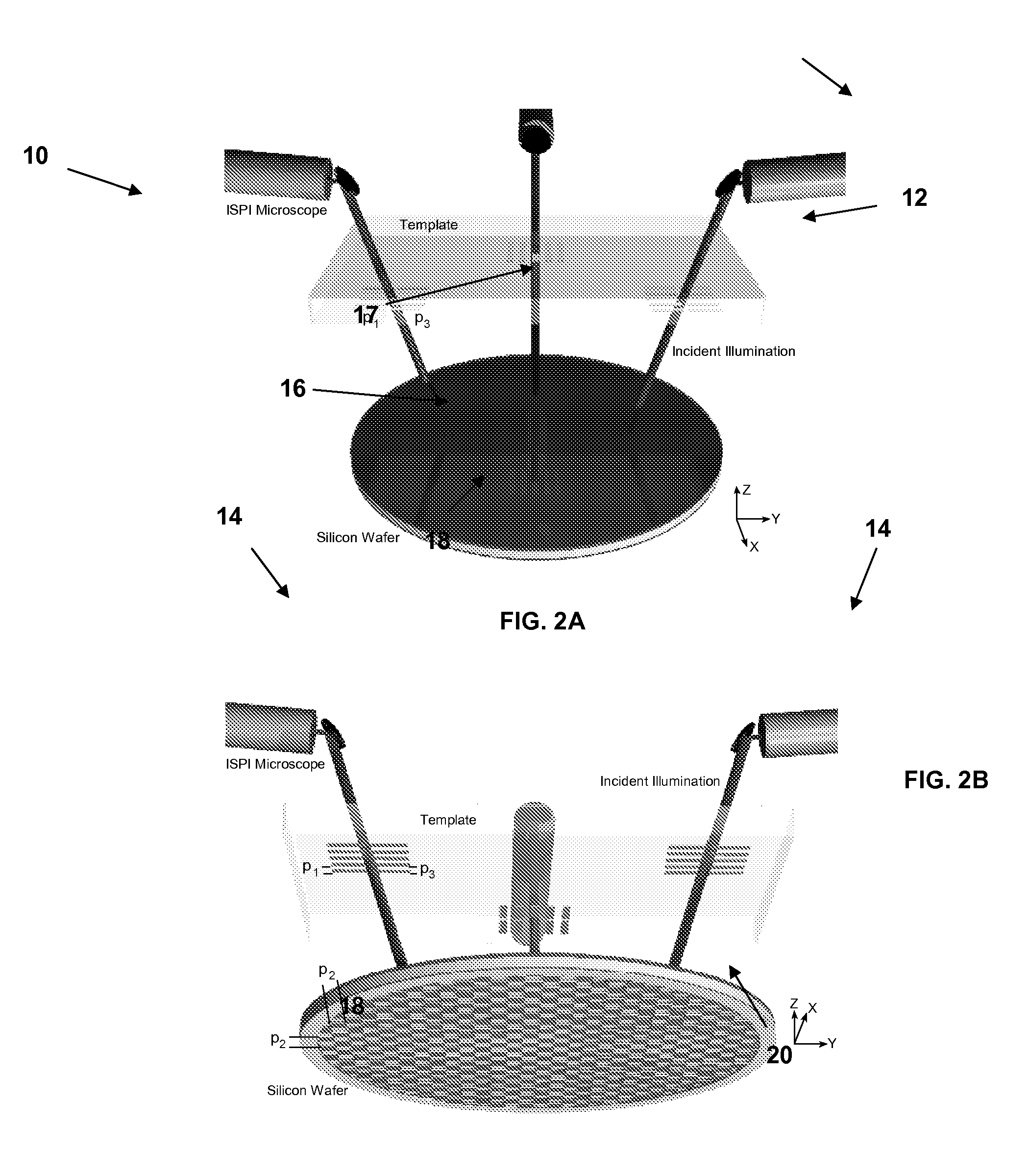
[0014] The invention relates to a technique for alignment and position measurement using marks that are embedded in a wafer, such as on the wafer backside, and occupy zero area on the wafer frontside and device patterning areas.
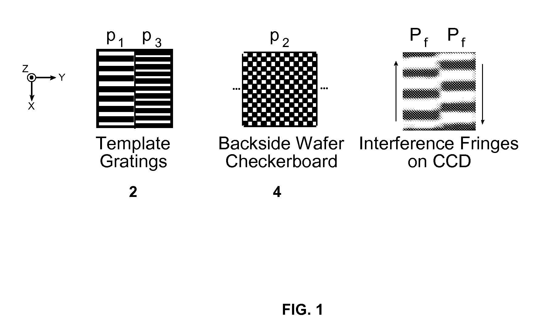
[0015] The invention uses grating and checkerboard patterns on two surfaces, such as on a template and embedded in a wafer, as illustrated in FIG. 1. The design of interferometric-spatial-phase imaging (ISPI) marks consists of markings 2 with period p1 and p3 on a template in proximity to a wafer with markings 4 with period p2. The checkerboard marks 4 typically cover the entire wafer backside and have a period of p2 in two orthogonal directions. FIG. 1 shows template gratings for detecting displacement along the X direction. Y detection is done with marks identical to the shown template marks 2, but in the orthogonal direction. X and Y detection are performed using the same checkerboard marks 4. The CCD image of the interference fringes that result from sup...
PUM
 Abstract
Description
Claims
Application Information