
Semiconductor device having a circular-arc profile on a silicon surface

a silicon surface and silicon-based technology, applied in the field of silicon-based semiconductor devices, can solve the problems of reducing affecting the reliability of the mos transistor, and unable to secure the gate width, and achieve the effect of widening the gate width

Active Publication Date: 2007-11-01
MICRON TECH INC
View PDF12 Cites 2 Cited by
  • Summary
  • Abstract
  • Description
  • Claims
  • Application Information

AI Technical Summary

Benefits of technology

[0010]It is an object of the present invention to provide a semiconductor device including MIS transistors having a larger gate width without causing degradation in the reliability of the MIS transistors.

Problems solved by technology

Reduction in the design rule of the semiconductor memory devices has recently been accelerated, which reduces the device area occupied by the MOS transistors, with the result that a sufficient gate width is difficult to secure.
A smaller thickness of the gate oxide film 14 causes a smaller withstand voltage thereof, to degrade the reliability of the MOS transistor.

Method used


Image

  • Semiconductor device having a circular-arc profile on a silicon surface
  • Semiconductor device having a circular-arc profile on a silicon surface
  • Semiconductor device having a circular-arc profile on a silicon surface

Examples


Embodiment Construction

[0026]Now, an exemplary embodiment of the present invention and a modification thereof will be described with reference to accompanying drawings, wherein similar constituent elements are designated by similar reference numerals throughout the drawings.

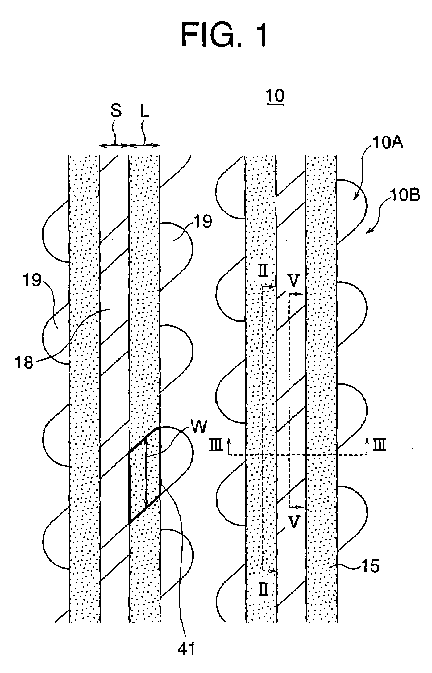
[0027]FIG. 1 is a top plan view showing part of the cell array area in a DRAM device illustrated as a semiconductor device according to an embodiment of the present invention. The DRAM device, generally designated at numeral 10, has element-forming regions 10A in each of which a pair of MOS transistors are formed and an element-isolating region 10B for isolating the element-forming regions 10A from one another.

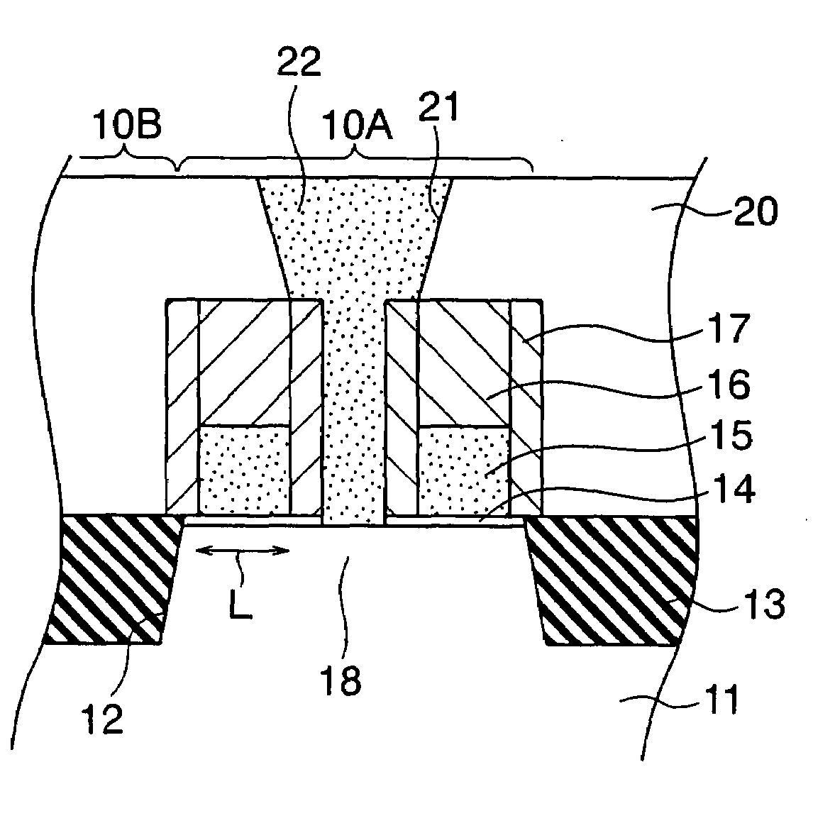
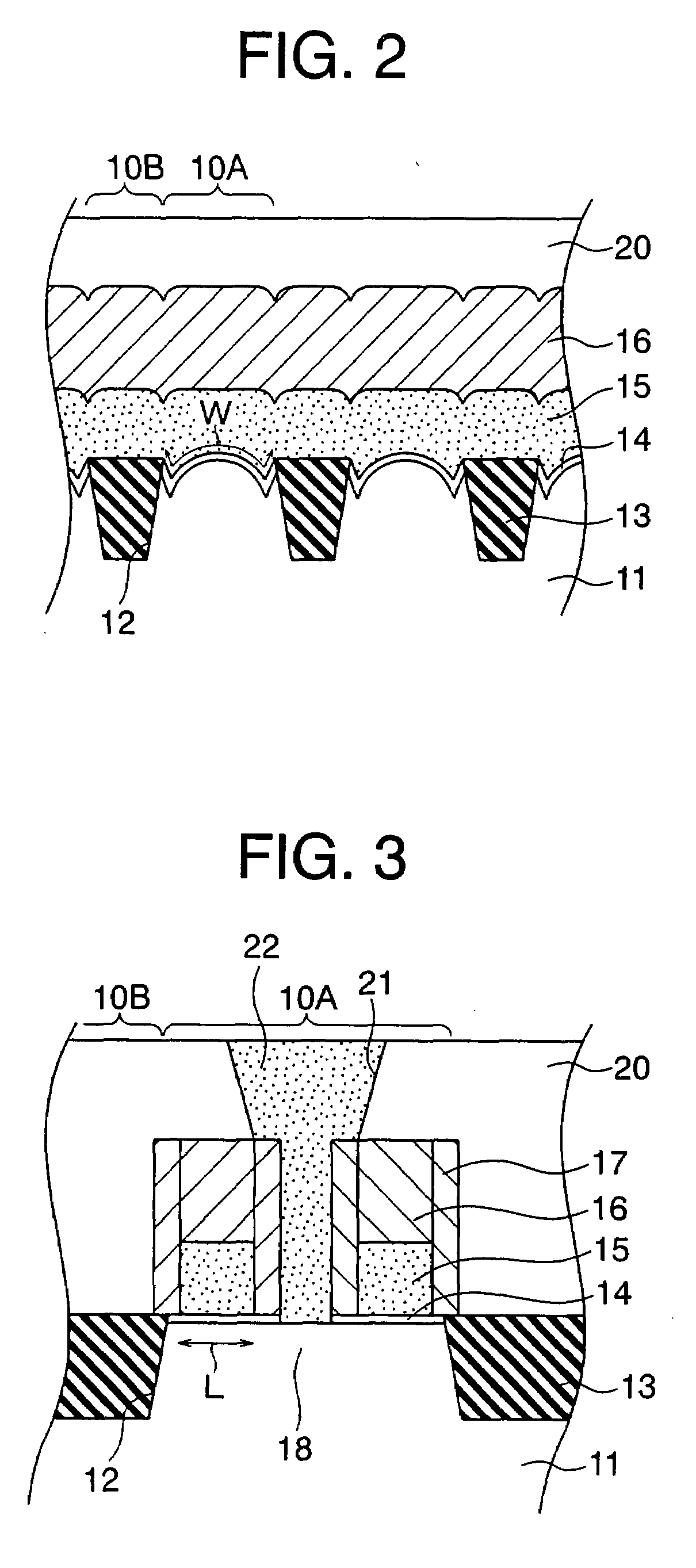
[0028]FIGS. 2 and 3 are sectional views taken along lines II-II and III-III, respectively, in FIG. 1. The semiconductor device 10 has a silicon substrate 11, and a trench 12 formed in a surface portion of the silicon substrate 11 to configure the element-isolating region 10B. A silicon oxide (SiO2) film 13 is embedded as an isola...


PUM


Abstract

A semiconductor device includes a shallow isolation trench (STI) structure on a silicon substrate for isolating element-forming regions from one another. The surface region of the silicon substrate in the element-forming regions, as viewed in the extending direction of the gate electrode lines, once falls and thereafter rises monotonically from the periphery toward the center of the element-forming regions.

Description

[0001]This application is based upon and claims the benefit of priority from Japanese patent application No. 2006-127349 filed on May 1, 2006, the disclosure of which is incorporated herein in its entirety by reference.BACKGROUND OF THE INVENTION[0002]1. Field of the Invention[0003]The present invention relates to a semiconductor device and a method for manufacturing the semiconductor device, and more particularly to a semiconductor device including therein MIS (Metal Insulator Semiconductor) transistors and a method for manufacturing the same.[0004]2. Description of the Related Art[0005]Semiconductor memory devices such as a DRAM (Dynamic Random Access Memory) device incorporate therein capacitors as storage elements and MOS (Metal Oxide Semiconductor) transistors for driving the capacitors. Reduction in the design rule of the semiconductor memory devices has recently been accelerated, which reduces the device area occupied by the MOS transistors, with the result that a sufficient ...

Claims


Application Information

Patent Timeline
Patent Type & Authority Applications(United States)
IPC IPC(8): H01L29/00
CPCH01L27/10873H01L29/0657H01L29/0696H01L29/78H01L29/41775H01L29/4236H01L29/41725H10B12/05
Inventor OHUCHI, MASAHIKO
Owner MICRON TECH INC
Learn More