Gan-based microwave power device with large gate width and manufacturing method thereof

a microwave power device and gate width technology, applied in the field of gan-based microwave power devices with a large gate width and manufacturing methods, can solve the problems of reducing signal gain, and reducing power added efficiency, and achieves high signal gain, high power added efficiency, and high electron mobility.

Active Publication Date: 2020-02-06
SOUTH CHINA UNIV OF TECH
View PDF0 Cites 0 Cited by
  • Summary
  • Abstract
  • Description
  • Claims
  • Application Information

AI Technical Summary

Benefits of technology

[0004]The objective of the present invention is to overcome the defects of the prior art described above, and from the viewpoint of optimizing the gate finger distribution of the device, to propose a GAN-based microwave power device with a large gate width and manufacturing method thereof, thereby improving the total output power and efficiency of the device, reducing the chip area, reducing the difficulty of process, and improving yield.
[0028]Compared with the prior art, the present invention has following advantages and technical effects.
[0029]The device is a GaN-based high electron mobility transistor based on AlGaN / GaN heterojunction. which forms a large gate width device structure of the fishbone-like drain electrode by optimizing the gate finger distribution, and avoids the problems such the phase shift of the electrical signal, the parasitic capacitance and so on, in the traditional multi-finger gate structures such as parallel gate and fishbone-like gate and so on. The device has a high signal gain, a high power added efficiency, and a high output power. At the same time, the manufacturing process of the device is simple, the chip area is saved, and the device has a good repeatability. The GaN-based microwave power device with the large gate width of the present invention is suitable for the fields such as high frequency, high power wireless communication, radar and so on.

Problems solved by technology

The more the number of gate fingers, the more serious this situation is, and the more the power added efficiency is reduced.
The disadvantage of the fishbone-like gate structure is that the air bridge of each drain terminal crosses over the gate and the source electrode, causing a large parasitic capacitance, resulting in a decrease in signal gain.
On the whole, the parallel gate structure and the fishbone-like gate structure improve the total power of the device, meanwhile, they also bring about problems such as decreased power added efficiency and decreased signal gain and so on.

Method used


Image

  • Gan-based microwave power device with large gate width and manufacturing method thereof
  • Gan-based microwave power device with large gate width and manufacturing method thereof
  • Gan-based microwave power device with large gate width and manufacturing method thereof

Examples


Embodiment Construction

[0032]The specific implementation of the present invention is further described below with reference to the accompanying drawings and embodiment, but the implementation and protection of the present invention are not limited thereto. It should be noted that, if any course or process parameters are not described in detail below, it can be achieved with reference to the prior art by those skilled in the art.

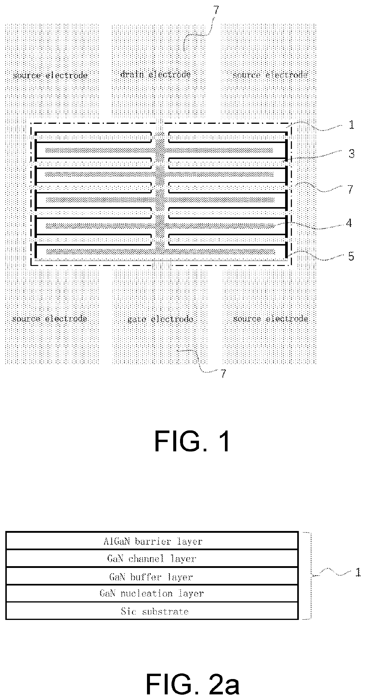
[0033]Referring to FIG. 1, a GAN-based microwave power device with a large gate width, includes: an AlGaN / GaN heterojunction epitaxial layer 1, a first dielectric layer 2 overlying the AlGaN / GaN heterojunction epitaxial layer, a strip-like source electrode 3, a drain electrode 4 distributed in a shape of a fishbone, a annular gate electrode 5, a second dielectric layer 6 separating upper and lower electrodes, and a interconnect metal electrode pad 7.

[0034]The AlGaN / GaN heterojunction epitaxial layer includes a substrate, a nitride nucleation layer, a nitride buffer layer, a GaN cha...


PUM

PropertyMeasurementUnit
thicknessaaaaaaaaaa
thicknessaaaaaaaaaa
thicknessaaaaaaaaaa

Abstract

The present invention provides a GaN-based microwave power device with a large gate width and manufacturing method thereof. The device includes an AlGaN / GaN heterojunction epitaxial layer, a first dielectric layer overlying the AlGaN / GaN heterojunction epitaxial layer, a strip-like source electrode, a drain electrode distributed in a shape of a fishbone, an annular gate electrode, a second dielectric layer separating upper and lower electrodes, and an interconnect metal electrode pad. The GaN-based microwave power device with the large gate width prepared according to the present invention, has a small phase shift of the signals, a small parasitic capacitance of the device, a high signal gain, high power added efficiency and a high output power. At the same time, the manufacturing process of the device is simple, the chip area is saved, and the device has a good repeatability.

Description

BACKGROUNDTechnical Field[0001]The present invention relates to the field of semiconductor device technology, and in particular to a GAN-based microwave power device with a large gate width and manufacturing method thereof, which can be used in the fields such as high frequency, high power wireless communication, radar, and so on.Description of Related Art[0002]With the development of modern weaponry, aerospace, nuclear power, communication technology, automotive electronics, and switching power supplies, higher requirements are placed on the performance of semiconductor devices. As a typical representative of wide bandgap semiconductor materials, GaN-based materials have characteristics such as a large width of bandgap, a high electron saturation drift velocity, high critical breakdown field strength, high thermal conductivity, good stability, corrosion resistance, radiation resistance, and so on, which can be used for fabricating high temperature, high frequency and high power ele...

Claims


Application Information

Patent Timeline
Patent Type & Authority Applications(United States)
IPC IPC(8): H01L29/423H01L29/417H01L29/778H01L29/20H01L29/66
CPCH01L29/41725H01L29/2003H01L29/4238H01L29/7786H01L29/66462H01L29/42316H01L29/7787H01L29/41758
Inventor WANG, HONGZHOU, QUANBIN
Owner SOUTH CHINA UNIV OF TECH
Why Eureka
Try Eureka