Method for operating non-volatile memory device

a non-volatile memory and operating method technology, applied in the direction of static storage, digital storage, instruments, etc., can solve the problems of insufficient data value determination threshold voltage distribution, difficult data state discrimination, and inability to achieve data value determination, so as to minimize the threshold voltage shift and the threshold voltage distribution change

Inactive Publication Date: 2007-11-22
SAMSUNG ELECTRONICS CO LTD
View PDF3 Cites 6 Cited by
  • Summary
  • Abstract
  • Description
  • Claims
  • Application Information

AI Technical Summary

Benefits of technology

[0013]Embodiments of the invention provide a method for removing electrons trapped in a tunnel insulating layer in order to minimiz

Problems solved by technology

In a case where the difference between a writing threshold voltage and an erase threshold voltage is relatively small, the resulting distribution of memory cell threshold voltages may be insufficient to allow data value determination.
While multi-level cells offer increased data density, they also pose additional difficulties in the bit-value deter

Method used


Image

  • Method for operating non-volatile memory device
  • Method for operating non-volatile memory device
  • Method for operating non-volatile memory device

Examples


Embodiment Construction

[0025]Embodiments of the invention will be described below in some additional detail with reference to the accompanying drawings. The present invention may, however, be embodied in many different forms and should not be constructed as being limited to only the embodiments set forth herein. Rather, these embodiments are presented as teaching examples.

[0026]In the figures, the dimensions of various layers and regions may have been exaggerated for purpose of clarity. It will also be understood that when a layer (or film) is referred to as being ‘on’ another layer or substrate, it can be directly on the other layer or substrate, or intervening layers may also be present. Throughout the drawings and the specification, like reference numerals refer to like or similar elements.

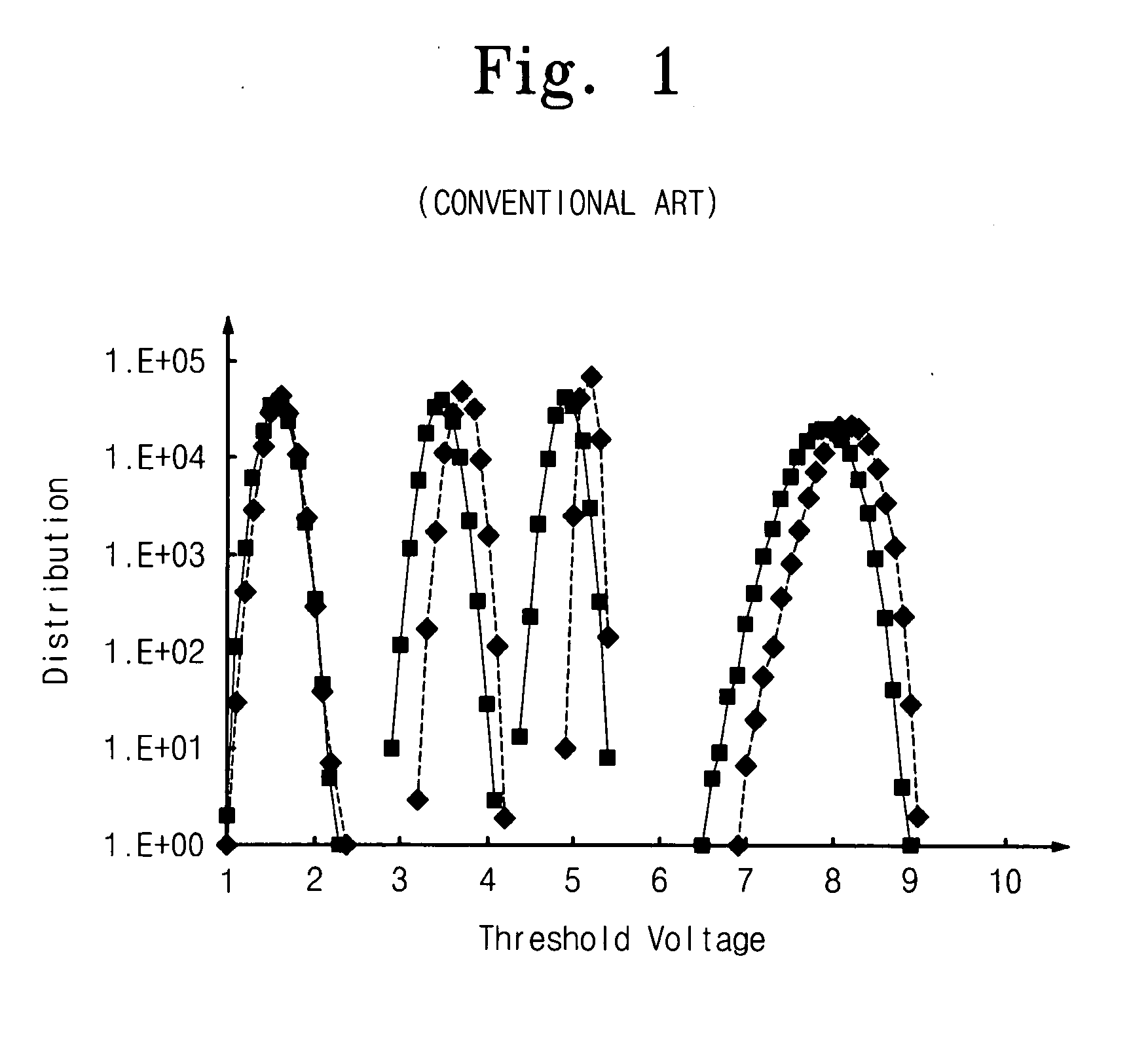
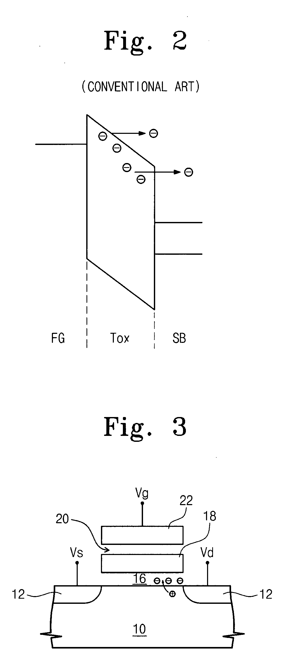
[0027]FIG. 3 is a schematic view illustrating a process of removing electrons trapped in a tunnel insulating layer through the injection of holes.

[0028]Referring to FIG. 3, the non-volatile memory device includes a s...


PUM


Abstract

A method of operating a non-volatile memory device is disclosed. The memory cell includes a channel region separating a source region and a drain region, a tunnel insulating layer, a charge storage layer, and a gate electrode formed over the channel region. The method includes applying a negative voltage to the gate electrode and applying a positive voltage to at least one of the source and drain regions to inject holes into the tunnel insulating layer and thereby remove electrons trapped in the tunnel insulating layer.

Description

CROSS-REFERENCE TO RELATED APPLICATIONS[0001]This U.S. non-provisional patent application claims priority under 35 U.S.C. §119 of Korean Patent Application No. 2006-45798, filed on May 22, 2006, the subject matter of which is hereby incorporated by reference.BACKGROUND OF THE INVENTION[0002]1. Field of the Invention[0003]The present invention relates to a method for operating a semiconductor device. More particularly, the invention relates to a more reliable method of operating a non-volatile semiconductor device.[0004]2. Description of the Related Art[0005]So-called flash memory is one common type of non-volatile memory. The flash memory device writes or erases data by supplying electrical charge to or removing electrical charge from a charge storage layer via a tunnel insulating layer. When negative charge is accumulated in the charge storage layer of a memory cell in its initial state, a corresponding threshold voltage for the constituent cell transistor increases. Alternately, w...

Claims


Application Information

Patent Timeline
IPC IPC(8): G11C11/34G11C16/04
CPCG11C11/5671G11C16/0483G11C16/345G11C16/3409G11C16/10
Inventor KIM, DAE-MANNKWON, WOOK-HYUNKIM, KI-NAMPARK, CHAN-KWANGSIM, SANG-PIL
Owner SAMSUNG ELECTRONICS CO LTD
Why Eureka
Try Eureka