Front-end processed wafer having through-chip connections

Inactive Publication Date: 2007-12-06
CUFER ASSET LTD LLC
View PDF99 Cites 2 Cited by
  • Summary
  • Abstract
  • Description
  • Claims
  • Application Information

AI Technical Summary

Benefits of technology

[0005]We have devised a way to minimize the risk and cost associated with the use of through-chip electrical connections in conjunction with device-bearing chips. By forming the through-chip connections on a blank wafer, the risk of damaging devices is advantageously eliminated (because there are no devices to damage). Moreover, in the event of a problem that renders the wafer unusable, the cost effect is also reduced because the wafer has not yet undergone any device creation or back-end processing procedures.

Problems solved by technology

For instance, some of these advantages are mutually contradictory, in that they cannot be simultaneously present in a single embodiment.

Method used


Image

  • Front-end processed wafer having through-chip connections
  • Front-end processed wafer having through-chip connections

Examples


Embodiment Construction

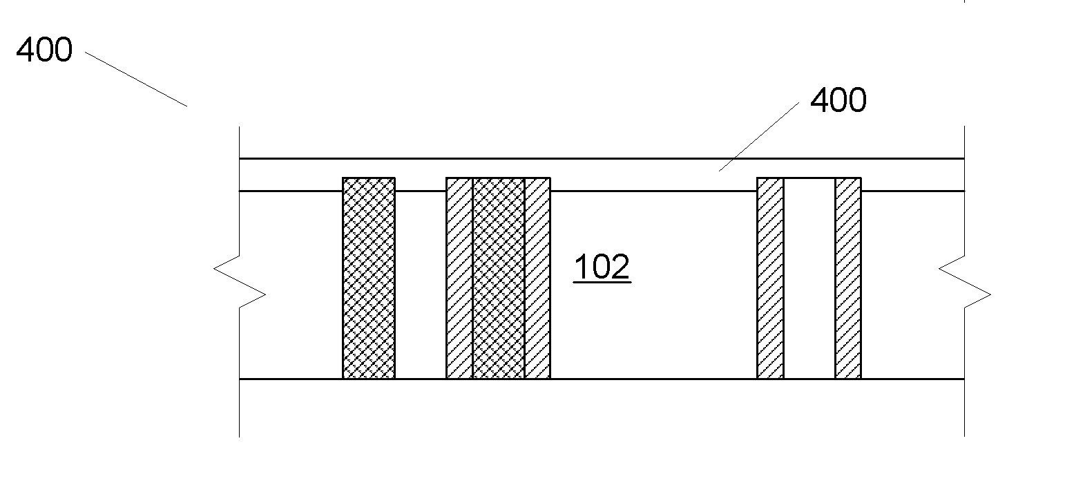
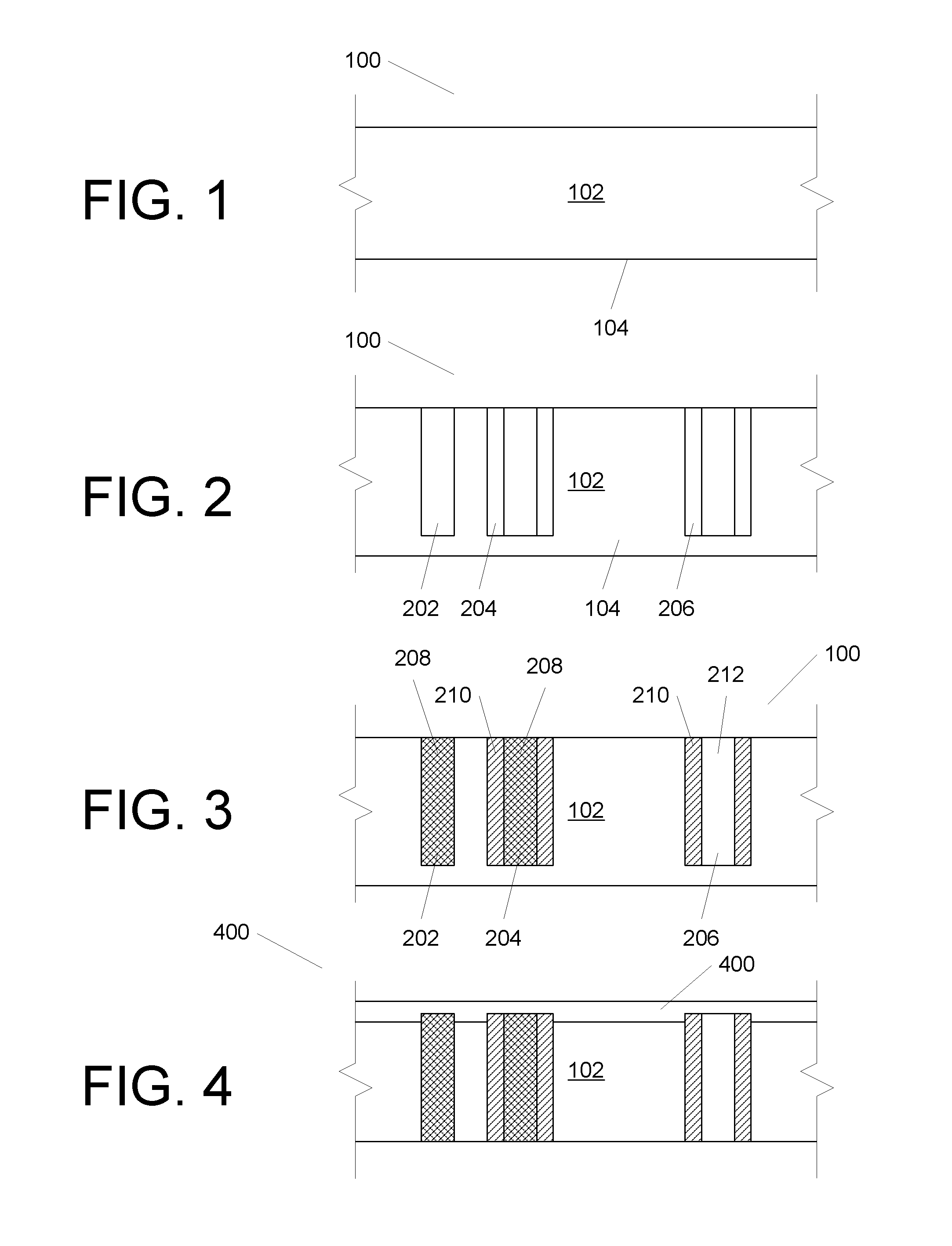
[0012]U.S. patent applications, Ser. Nos. 11 / 329,481, 11 / 329,506, 11 / 329,539, 11 / 329,540, 11 / 329,556, 11 / 329,557, 11 / 329,558, 11 / 329,574, 11 / 329,575, 11 / 329,576, 11 / 329,873, 11 / 329,874, 11 / 329,875, 11 / 329,883, 11 / 329,885, 11 / 329,886, 11 / 329,887, 11 / 329,952, 11 / 329,953, 11 / 329,955, 11 / 330,011 and 11 / 422,551, incorporated herein by reference describe various techniques for forming small, deep vias in, and electrical contacts for, semiconductor wafers. Our techniques allow for via densities and placement that was previously unachievable and can be performed on a chip or wafer scale.

[0013]In cases where it is desirable to create through-chip electrical connections, but minimize the risks involved with fully processed wafers (i.e. device bearing wafers), the following approach can be used.

[0014]In summary overview, the approach straightforwardly involves forming vias in a blank wafer at the locations where they should be relative to devices that would be on the wafer once front end proce...


PUM


Abstract

A method involves forming vias in a blank semiconductor wafer, making at least some of the vias in the blank semiconductor wafer electrically conductive, and performing front end processing on the blank wafer so as to create devices on the wafer that are connected to the electrically conductive vias.

Description

CROSS REFERENCE TO RELATED APPLICATIONS[0001]This application is a continuation-in-part of U.S. patent application Ser. No. 11 / 422,551, and further claims the benefit of priority, pursuant to 35 U.S.C. 119(e), of U.S. Provisional Application Ser. No. 60 / 882,671 filed Dec. 29, 2006. The entirety of both are incorporated herein by reference as if fully set forth herein.FIELD OF THE INVENTION[0002]The present invention relates to semiconductors and, more particularly, to electrical connections for such devices.BACKGROUND[0003]It is sometimes desirable to be able to form electrical connections through a chip to facilitate connecting it to another element in an efficient manner. In many cases, this means use of vias and involve connections that are made near the devices of chips as opposed to forming connections at or near the periphery of the chip, as is done with conventional methods.[0004]One drawback to using through-chip vias on fully processed (i.e. device-bearing) chips is that fu...

Claims


Application Information

Patent Timeline
IPC IPC(8): H01L21/768
CPCH01L21/76898
Inventor TREZZA, JOHN
Owner CUFER ASSET LTD LLC
Why Eureka
Try Eureka