

Method for producing si1-ygey based zones with different contents in ge on a same substrate by condensation of germanium
a technology of germanium and ge, applied in the direction of electrical equipment, instruments, material analysis, etc., can solve the problems of increased difficulty, increased difficulty, and inability to achieve optimal transistor performance in such a structur
- Summary
- Abstract
- Description
- Claims
- Application Information
AI Technical Summary
Problems solved by technology
Method used
Image

Examples
Embodiment Construction
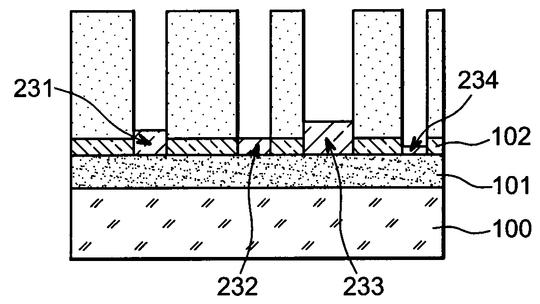
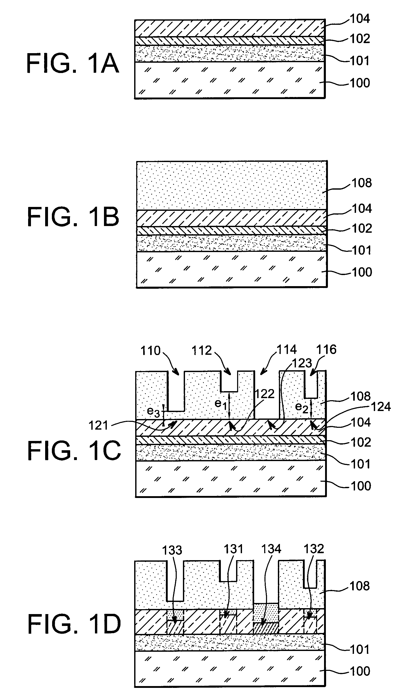
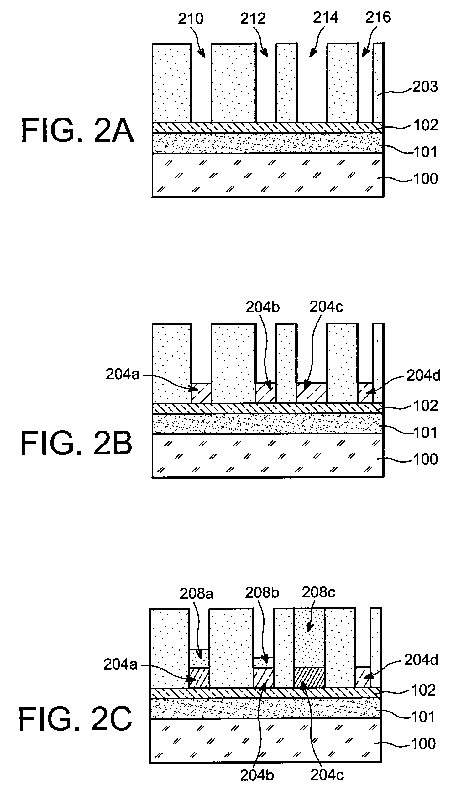
[0007]The invention relates to a method for producing a microelectronic device including a plurality of based Si1-yGey semi-conducting zones (where 0<y≦1) with different respective contents in Germanium.
[0008]In one aspect, the invention relates to a method comprising steps of:
[0009]a) formation on a substrate covered with a plurality of Si1-yGey based semi-conducting zones (where 0<x< and x<y) and identical compositions, of at least one mask comprising a set of masking blocks, wherein the masking blocks respectively cover at least one semi-conducting zone of said plurality of semi-conducting zones, wherein several of said masking blocks have different thicknesses and / or are based on different materials,
[0010]b) oxidation of the semi-conducting zones of said plurality of semi-conducting zones through said mask.
[0011]The masking blocks thicknesses and / or materials is designed to induce a delay with oxidation, this oxidation being carried out to lead to the formation of the aforesaid ...
PUM
 Abstract
Description
Claims
Application Information