Power semiconductor device and method for its production

Active Publication Date: 2007-12-13
INFINEON TECH AG
View PDF11 Cites 78 Cited by
  • Summary
  • Abstract
  • Description
  • Claims
  • Application Information

AI Technical Summary

Benefits of technology

[0036] This ensures that the second wiring layer remains protected from mechanical and chemical attacks and damage. However, even before the second layer of plastic of the package is introduced, further semiconductor chips and/or passive components may be mounted with their electrodes on the plate regions of the connecting elements by means of diffusion solder, soft solder or electrically conducting adhesive. This has the advantage that it is then possible in turn for a further layer of plastic of the package to be applied and then patterned and for contact vias then to be introduced into it and plate regions to be created on its plane-parallel upper side, which regions can in turn be made available for their part for further stackable semiconductor chips. However, this requires that two further layers of plastic must be applied, namely, one which embeds the stacked further semiconductor chip and a further one which covers the connecting

Problems solved by technology

These have the disadvantage that they require a certain bonding loop height, with the result that the device package cannot be reduced in size any further.
However, this wiring solution has the disadvantage that the method of produc

Method used


Image

  • Power semiconductor device and method for its production
  • Power semiconductor device and method for its production
  • Power semiconductor device and method for its production

Examples


first embodiment

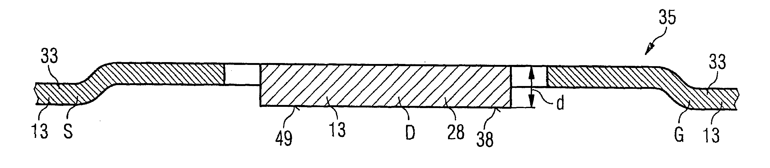
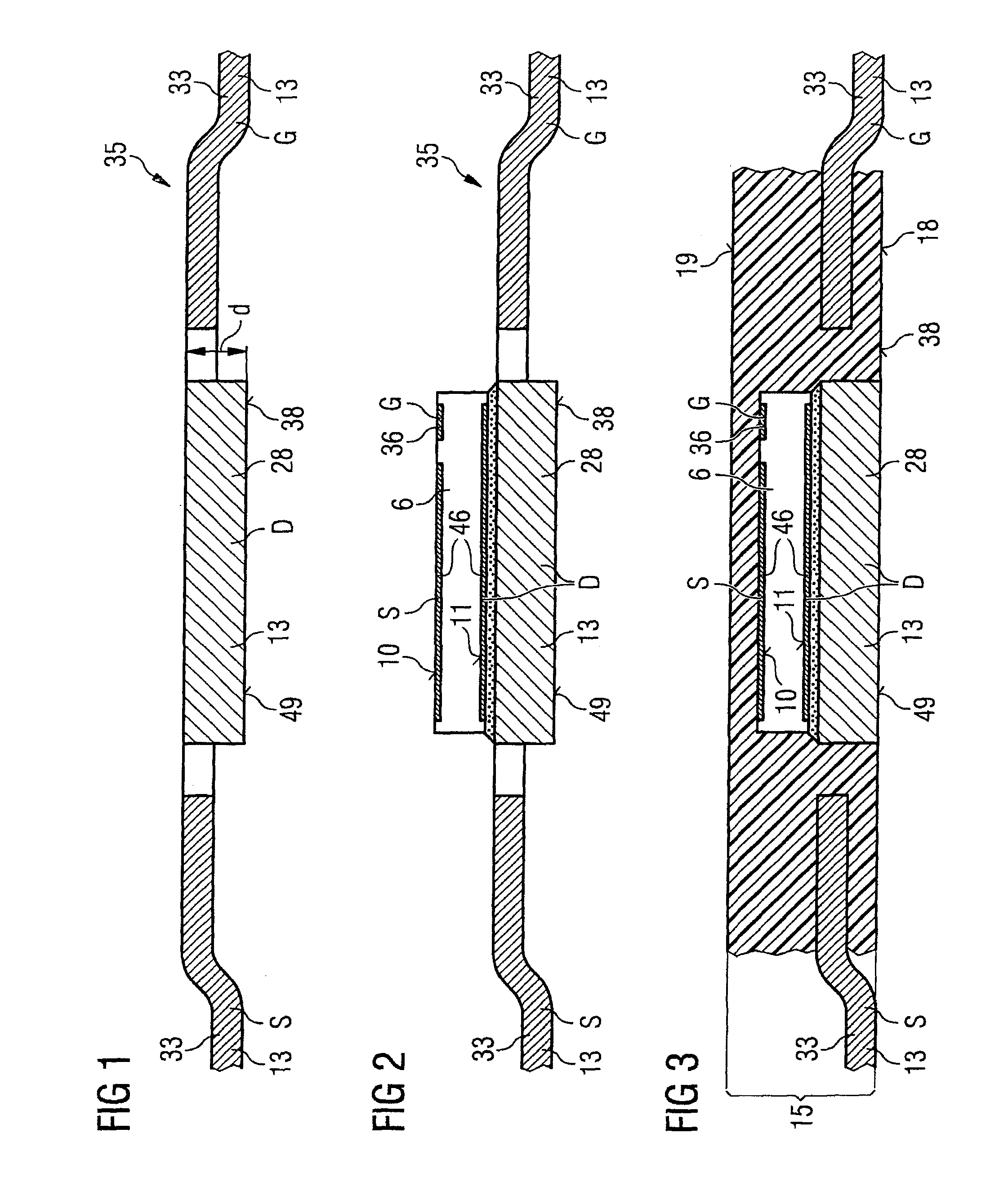
[0053] FIGS. 1 to 7 show schematic cross sections through components in the production of a power semiconductor device 1 according to the invention. Components with the same functions are identified in the subsequent figures by the same designations and are not explained more than once.

[0054]FIG. 1 shows a schematic cross section through a leadframe 35. Such leadframes 35 may, depending on the type of package, be differently patterned. There are leadframes which have in addition to a chip carrier 28, as is shown in FIG. 1, external leads 33, which are dimensioned in such a way that they provide external contact areas on the underside and / or on edge sides of a plastic package 14 after completion. Other leadframes 35 are intended to allow leads 33 to protrude as external contacts 13 from the plastic package of the power semiconductor device on the edge sides. In this embodiment of the invention, a leadframe 35 is used, having external contacts 13 which have the form of external leads ...

second embodiment

[0063] In the production of the second layer of plastic 16, it is mounted with its underside 20 on the first layer of plastic 15. With the plate regions 27 of the connecting elements 12 being formed with different thicknesses, it is also possible that the electrodes of the power semiconductor chip 6 can be accessed from the surface 32 of the power semiconductor device, which is formed by the upper side 21 of the second layer of plastic 16. This is shown in the invention.

[0064]FIG. 8 shows a schematic cross section through a power semiconductor device 2 according to a second embodiment of the invention. Components with the same functions as in the previous figures are identified by the same designations and are not explained in any more detail. The difference between the second embodiment of the invention according to FIG. 8 and the first embodiment of the invention according to FIG. 7 is that the plate regions 27 of the wiring elements 12 have different thicknesses S1 and S2. While ...

third embodiment

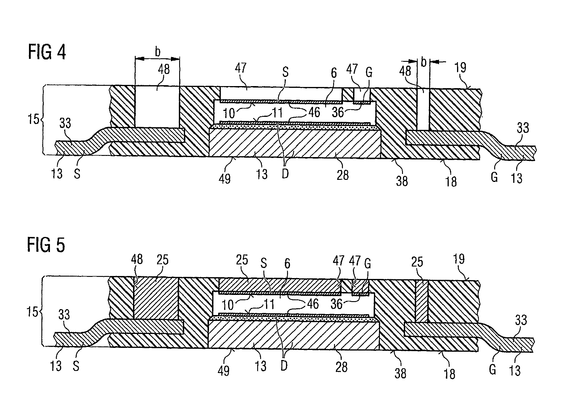
[0065]FIG. 9 shows a schematic cross section through a power semiconductor device 3 according to the invention. The difference from the previous embodiments of the invention is that the source electrode S of the power semiconductor chip 6 is connected to the chip carrier 28 in a first layer of plastic 15 by means of a plate region 27 of a connecting element 12 with contact vias 25. The power semiconductor chip 6 itself is arranged in a second layer of plastic 16 and is covered by a third layer of plastic 17.

[0066] Arranged in the third layer of plastic 17 is a further wiring layer 34, which has a further plate region 27 of a connecting element 12. The further plate region 27 of the connecting element 12 in the third layer of plastic 17 forms a connection between the drain electrode D on the back side 11 of the power semiconductor chip 6 and a lead 33 by means of a contact via 26 and a plate region 27 in the second layer of plastic 16 as well as by means of a further contact via 25. ...


PUM


Abstract

A power semiconductor device and a method for its production. The power semiconductor device has at least one power semiconductor chip, which has on its top side and on its back side large-area electrodes. The electrodes are electrically in connection with external contacts by means of connecting elements, the power semiconductor chip and the connecting elements being embedded in a plastic package. This plastic package has a number of layers of plastic, which are pressed one on top of the other and have plane-parallel upper sides. The connecting elements are arranged on at least one of the plane-parallel upper sides, between the layers of plastic pressed one on top of the other, as a patterned metal layer and are electrically in connection with the external contacts by means of contact vias through at least one of the layers of plastic.

Description

FIELD OF THE INVENTION [0001] Embodiments of the invention relate to a power semiconductor device and to a method for its production. The power semiconductor device has at least one power semiconductor chip, which has on its top side and on its back side not only small-area control electrodes but also large-area power electrodes. The electrodes are electrically in connection with external contacts by means of connecting elements, and the power semiconductor chip and the connecting elements being embedded in a plastic package. BACKGROUND [0002] Conventional power semiconductor devices, which have one or more power semiconductor chips, have electrical connecting elements which electrically connect top side and back side of the power semiconductor chip to external contact areas of the device. The external contact areas may be provided by a leadframe or on a wiring substrate. The electrical connecting elements may be provided by bonding wires, which extend between the top side of the po...

Claims


Application Information

Patent Timeline
IPC IPC(8): H01L23/48
CPCH01L23/49524H01L2924/1305H01L23/49562H01L23/49575H01L23/49861H01L23/5389H01L24/24H01L24/82H01L25/071H01L2224/24226H01L2224/32245H01L2224/48465H01L2224/48472H01L2224/73265H01L2224/73267H01L2224/82039H01L2224/83801H01L2224/8382H01L2224/8384H01L2224/83855H01L2924/01013H01L2924/01029H01L2924/01082H01L2924/10253H01L2924/13055H01L2924/13091H01L23/49537H01L2924/13062H01L2924/1306H01L2224/48091H01L2924/014H01L2924/01068H01L2924/01033H01L2924/01019H01L2224/48247H01L24/48H01L2924/01005H01L2924/00014H01L2924/00012H01L2924/00H01L2924/351H01L2924/181H01L24/73H01L2224/83825H01L2224/8385H01L2224/06181H01L2224/0603H01L24/25H01L24/32H01L2224/73221H01L24/40H01L2224/40091H01L2224/40225H01L2224/45099H01L2224/45015H01L2924/207H01L2224/84H01L2224/37099H01L2224/40245H01L2224/40H01L24/37H01L24/41H01L2224/371
Inventor OTREMBA, RALFSTRACK, HELMUT
Owner INFINEON TECH AG
Why Eureka
Try Eureka