AC coupled parameteric test probe

a test probe and parameter technology, applied in the field of test probes, can solve the problems of causing damage to the dut being fabricated and creating debris, and achieve the effect of increasing signal coupling

Inactive Publication Date: 2007-12-27
FORMFACTOR INC
View PDF28 Cites 118 Cited by
  • Summary
  • Abstract
  • Description
  • Claims
  • Application Information

AI Technical Summary

Benefits of technology

[0007]According to some embodiments of the present invention, a system is provided to electromagnetically couple a test signal between a test probe and components of an integrated circuit (IC) on a semiconductor substrate. In at least some embodiments, the probe has a dielectric insulating material tip. Testing using the probe with a dielectric tip includes contacting the substrate with the dielectric insulating material tip of the probe when test signals are electromagnetically coupled by capacitive or inductive coupling between the probe and components of t

Problems solved by technology

During testing, contact made between the bond pads and resilient probes of the test system can cause damage to the DUT being fabricated.
Fu

Method used


Image

  • AC coupled parameteric test probe
  • AC coupled parameteric test probe
  • AC coupled parameteric test probe

Examples


Embodiment Construction

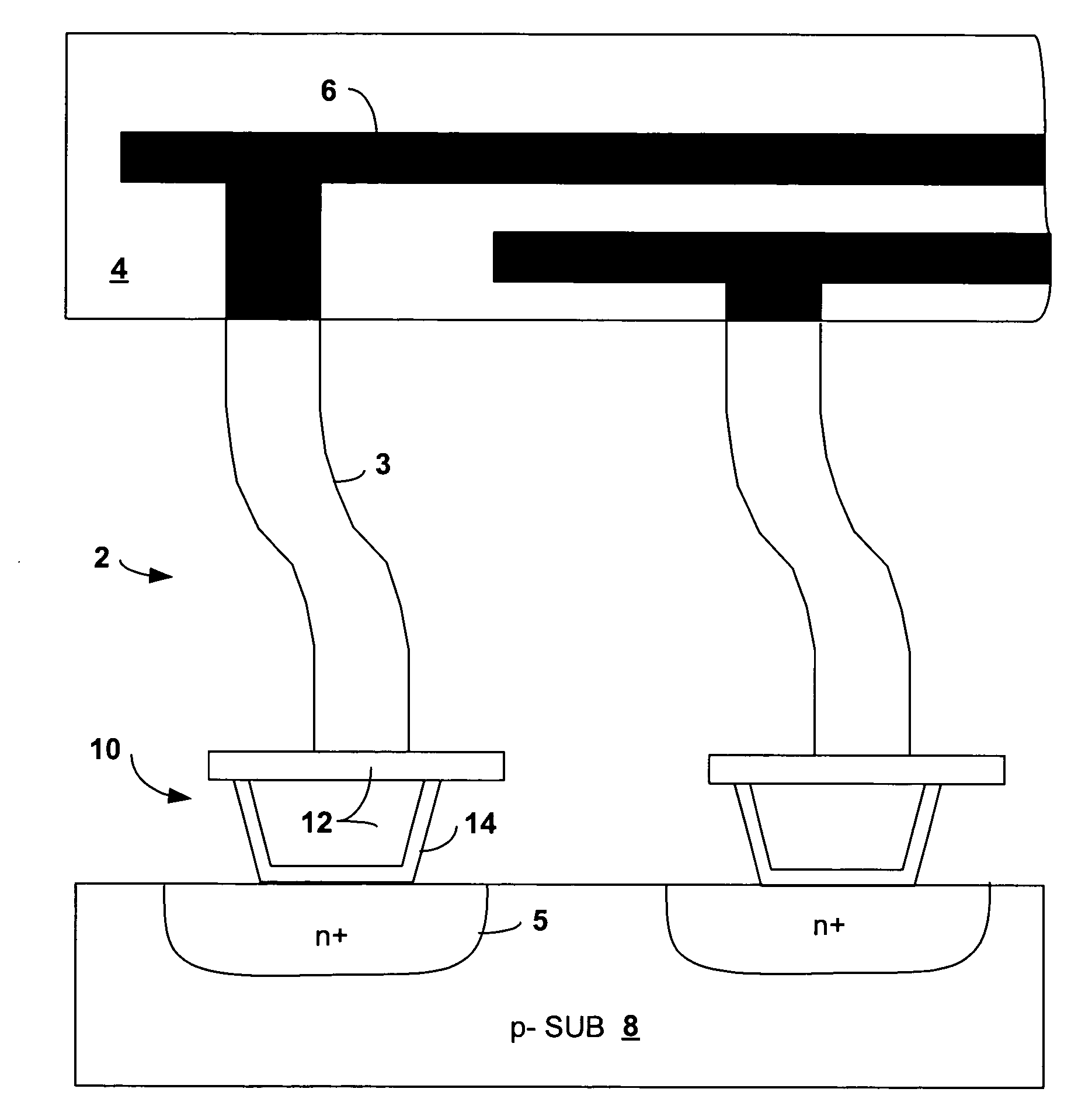
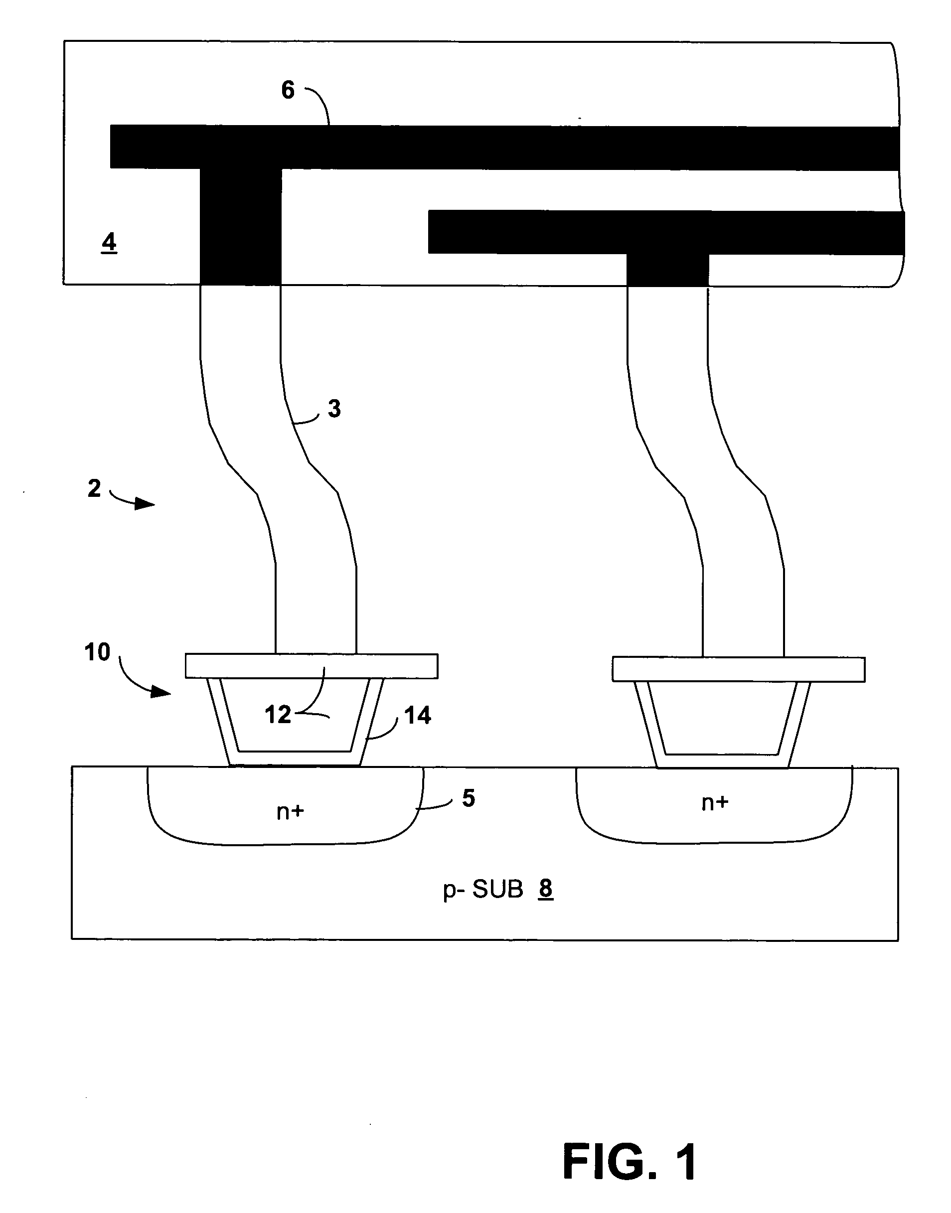
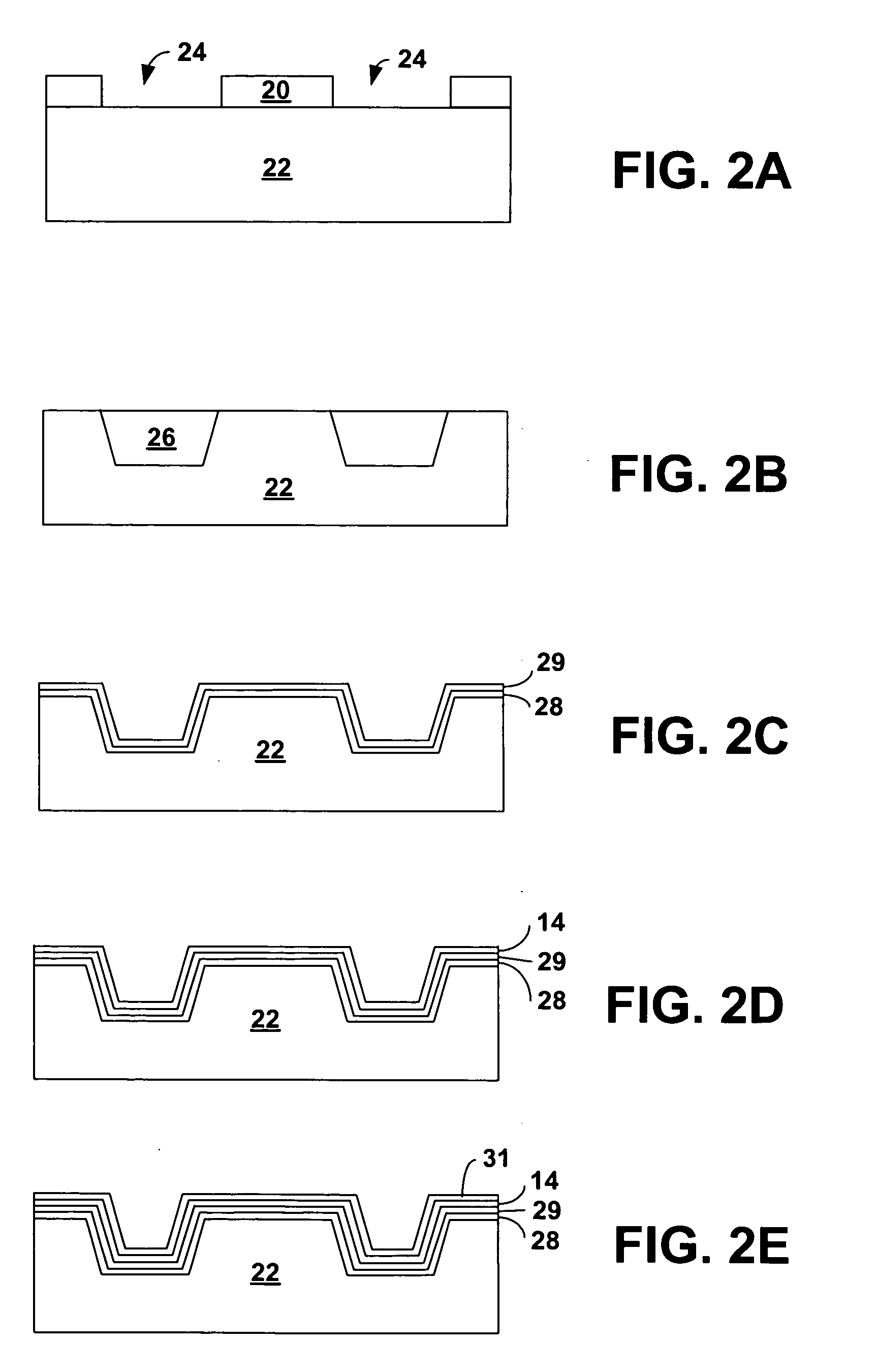
[0027]FIG. 1 shows exemplary probes attached to a probe card with capacitive coupling according to some embodiments of the present invention. The probes 2 are shown in the embodiments of FIG. 1 as compliant spring wire probes. The probes 2 are connected to a substrate, such as space transformer 4. The space transformer 4 forms part of a probe card assembly that transfers test signals between a test system (not shown) and the probes 2. The space transformer 4 can include traces 6 that redistribute lines from a pitch where the probes 2 are connected to connectors provided at a different pitch.

[0028]The probes 2 can be compliant spring wire probes. Such compliant spring probes can include a wire member made from a flexible conductive material. Details of fabrication of the wire probes 2 is provided in U.S. Pat. No. 5,476,211, entitled “Method of Manufacturing Electrical Contacts, Using a Sacrificial Member,” and U.S. Pat. No. 6,049,976 entitled “Method of Mounting Free-Standing Resilie...


PUM


Abstract

A probe for contacting and testing ICs on a semiconductor device includes a dielectric insulating material tip. The dielectric tip does not contaminate the surface being probed unlike metal probe tips. A contact scrub is further not required with signals being capacitively or inductively coupled from the probe tip to the IC. Testing can be performed during early fabrication steps of the wafer without the need for applying a metalization layer to the wafer to form bond pads. Testing can be performed by inductively coupling an AC signal to the probe tip, with coupling enhanced by including a magnetic material in the dielectric probe tip. Using an AC test signal enables testing of ICs without requiring separate power and ground connections.

Description

BACKGROUND[0001]1. Technical Field[0002]Embodiments of the present invention relate to components used to test integrated circuit devices under test (DUTs), either on a wafer, or diced up into individual dies. More particularly, embodiments of the present invention relate to test probes used to electrically connect a test system to electrical contact pads of the DUTs.[0003]2. Related Art[0004]Test systems to test DUTs during fabrication of a wafer typically include a test system controller that applies signals through channels of a probe card supporting test probes. The test probes are typically resilient to reduce damage to the wafer and the probes themselves during testing. To perform testing, the probes are brought into contact with conductive bond pads of DUTs formed on the wafer. In some cases, similar testing can be performed with a test system and probe card to test dies after the dies have been cut out from the wafer, but before wires are bonded to bond pads of DUTs on the d...

Claims


Application Information

Patent Timeline
IPC IPC(8): G01R31/02
CPCG01R1/06727G01R31/3025G01R1/06711G01R1/07G01R1/067G01R1/073G01R31/26H01L22/00
Inventor ELDRIDGE, BENJAMIN N.SPORCK, A. NICHOLASMILLER, CHARLES A.
Owner FORMFACTOR INC
Why Eureka
Try Eureka