Photonic Devices Monolithically Integrated with Cmos

a photonic device and monolithic technology, applied in semiconductor devices, diodes, electrical apparatus, etc., can solve the problems of reducing the external power efficiency severely, unable to take advantage of practical applications, and low efficiency

Active Publication Date: 2008-01-03
QUANTUM SEMICON
View PDF16 Cites 40 Cited by
  • Summary
  • Abstract
  • Description
  • Claims
  • Application Information

AI Technical Summary

Benefits of technology

[0007] An object of the present invention is a new process architecture for the fabrication of photonic devices, that is compatible with sub-micron and sub-100 nm CMOS technologies and improves the intrinsic and extrinsic efficiencies of light emission by avalanching junctions.

Problems solved by technology

Even though there has been ample experimental evidence since the 1950's that silicon can emit light, the efficiency has always been very low: roughly only 1 in 107 recombinations across the bandgap emit light.
In either case, the location which emits light can be hundreds of nanometers away from the substrate surface, and consequently photons with energy larger than the minimum bandgap of the substrate are absorbed, thereby severely reducing the external power efficiency.
For all the reasons mentioned above, band-structure, device design, and process architecture, it has been impossible to take advantage for practical applications, of light emission from silicon junctions operated in the avalanche mode.
On the other hand, conventional CMOS technology is not amenable to the integration of other semiconductor materials for the purpose of bandgap engineering of pn-junctions.
For this reason full monolithic integration of efficient light emitting devices with CMOS has not been possible.

Method used


Image

  • Photonic Devices Monolithically Integrated with Cmos
  • Photonic Devices Monolithically Integrated with Cmos
  • Photonic Devices Monolithically Integrated with Cmos

Examples


Embodiment Construction

[0061] 1. Method of Fabrication

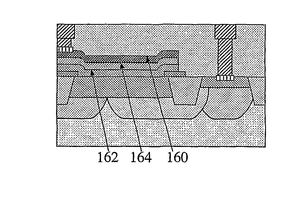
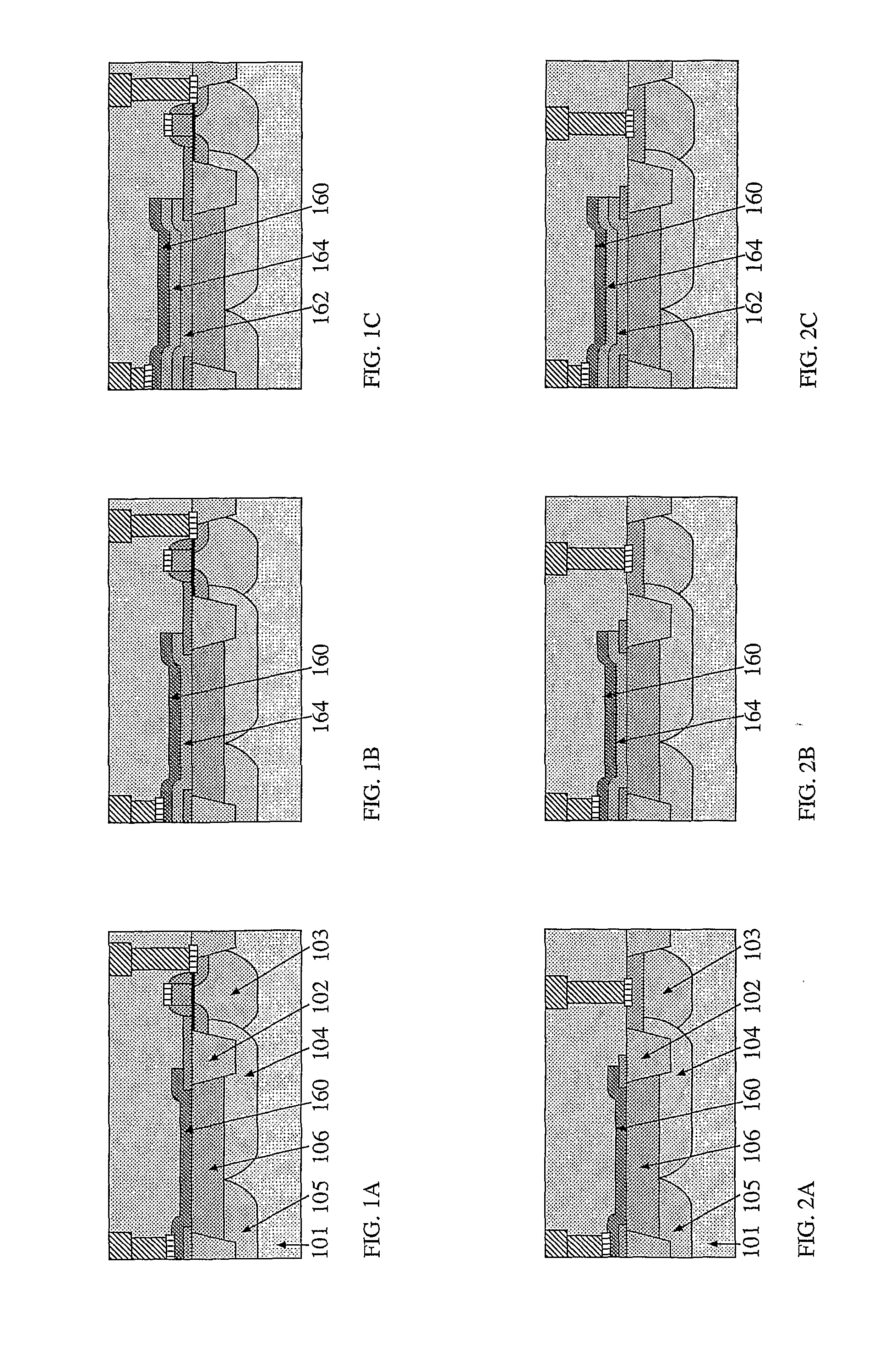
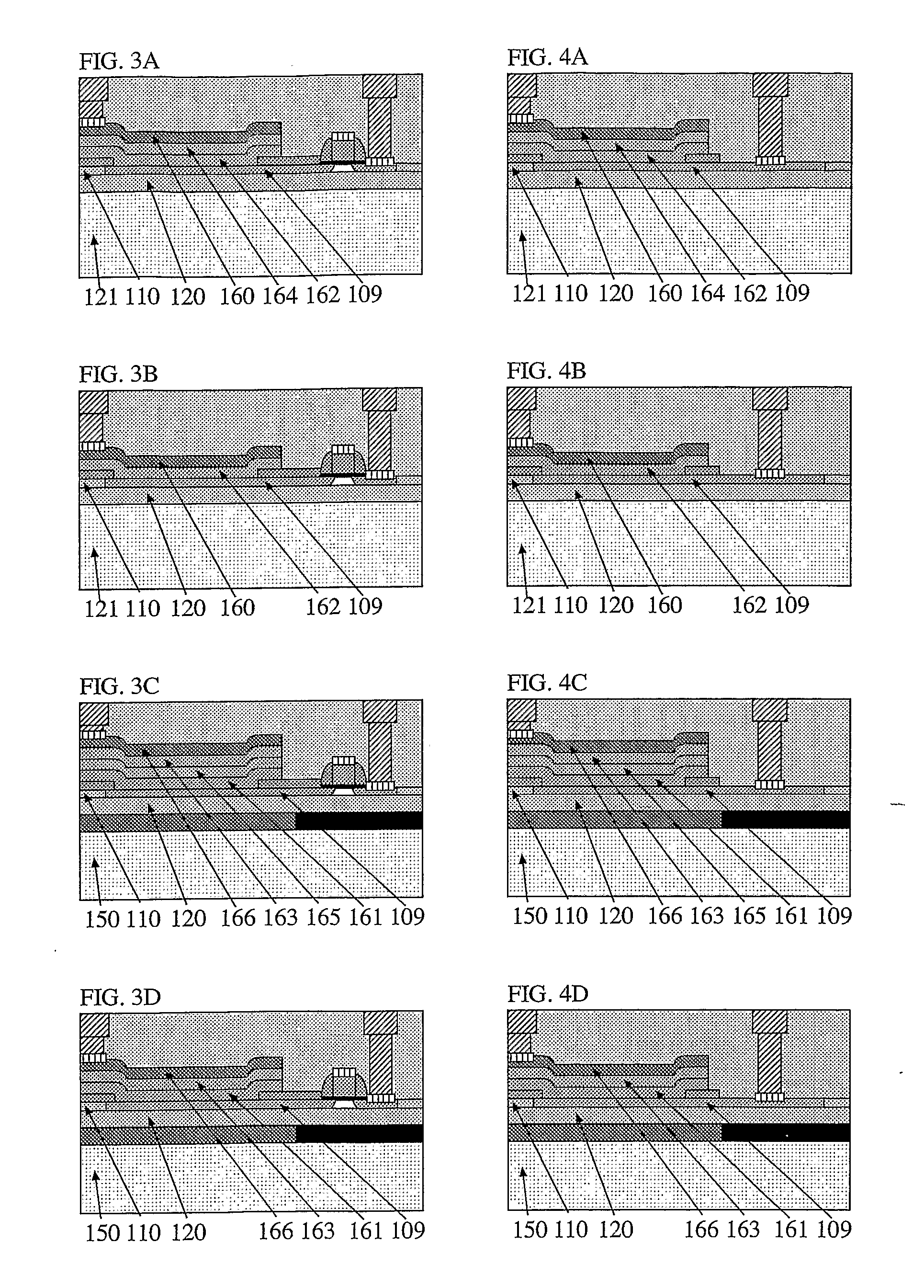
[0062] The present invention makes use of the fabrication architecture and process flows disclosed in WO 2002 / 33755 which covers the fabrication of Avalanche Photo-Diodes (APDs) with epitaxially grown active layers, monolithically integrated with bulk CMOS devices. The fundamental advantage of that fabrication architecture is that some of the active layers of the APDs are epitaxially deposited on CMOS active areas, immediately adjacent to MOSFETs, thereby resulting in a very compact monolithic integration with CMOS. Because some of the active layers are epitaxial layers deposited on a silicon surface (active area), it is possible to have materials that are epitaxially compatible with silicon, other than silicon itself.

[0063] Similarly to WO 2002 / 33755 and WO 2004 / 027879, the method of fabrication of the present invention, follows the standard CMOS process flow until the formation of silicide layers. Ideally the epitaxial deposition takes place after ...


PUM


Abstract

Photonic devices monolithically integrated with CMOS are disclosed, including sub-100nm CMOS, with active layers comprising acceleration regions, light emission and absorption layers, and optional energy filtering regions. Light emission or absorption is controlled by an applied voltage to deposited films on a pre-defined CMOS active area of a substrate, such as bulk Si, bulk Ge, Thick-Film SOI, Thin-Film SOI, Thin-Film GOI.

Description

BACKGROUND OF THE INVENTION [0001] The present invention relates to light emission from semiconductor junctions in general, and in particular when those junctions are operated in the avalanche mode, as the active regions of Avalanche Light Emitting Diodes (ALEDs), thereby enabling light emission from indirect bandgap materials. It relates to the design of device layers and layout, as well as the method of fabrication, suitable for monolithic integration of ALEDs with sub-micron and sub-100 nm CMOS technologies, forming “Light Emitting Elements” (hereafter referred to as LIXELs). LIXELs can be implemented with Silicon bulk substrates, Thick-Film SOI substrates, or ultra-thin-film Silicon-On-Insulator (SOI) substrates, as well as with Germanium bulk substrates or ultra-thin-film Germanium-On-Insulator (GOI) substrates. Thin-Film GOI substrates are good candidates to be the used for sub-45 nm CMOS technology. [0002] In the early years of semiconductor technology, it was noticed that si...

Claims


Application Information

Patent Timeline
Patent Type & Authority Applications(United States)
IPC IPC(8): H01L33/00H01L29/06
CPCH01L27/14603H01L27/14643H01L27/15H01L31/02027H01L31/1075H01L27/142H01L31/107Y02E10/547H01L27/1443H01L31/035236H01L31/18H01L33/0041H01L33/0054H01L33/06H01L33/34
Inventor AUGUSTO, CAROLS J.R.P.
Owner QUANTUM SEMICON
Why Eureka
Try Eureka