

Device manufacturing method
a technology of lithographic apparatus and manufacturing method, applied in the direction of electrical apparatus, printers, instruments, etc., can solve problems such as localized lens heating problems, and achieve the effect of improving process latitude and/or more uniform lens heating
- Summary
- Abstract
- Description
- Claims
- Application Information
AI Technical Summary
Benefits of technology
Problems solved by technology
Method used
Image


Examples
embodiments
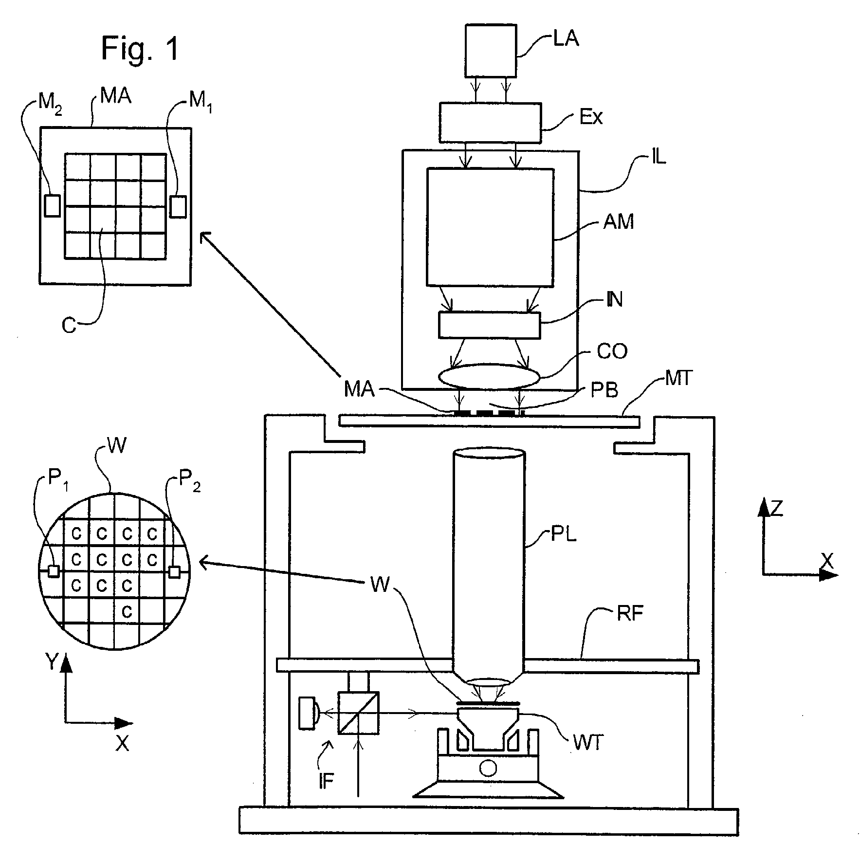
[0038]FIG. 1 schematically depicts a lithographic apparatus according to a particular embodiment of the invention. The apparatus comprises: [0039] an illumination system (illuminator) IL for providing a projection beam PB of radiation (e.g., UV radiation or DUV radiation). [0040] a first support structure (e.g., a mask table) MT for supporting patterning means (e.g., a mask) MA and connected to first positioning means PM for accurately positioning the patterning means with respect to item PL; [0041] a substrate table (e.g., a wafer table) WT for holding a substrate (e.g., a resist-coated wafer) W and connected to second positioning means PW for accurately positioning the substrate with respect to item PL; and [0042] a projection system (e.g., a refractive projection lens) PL for imaging a pattern imparted to the projection beam PB by patterning means MA onto a target portion C (e.g., comprising one or more dies) of the substrate W.
[0043] As here depicted, the apparatus is of a tran...
embodiment 2
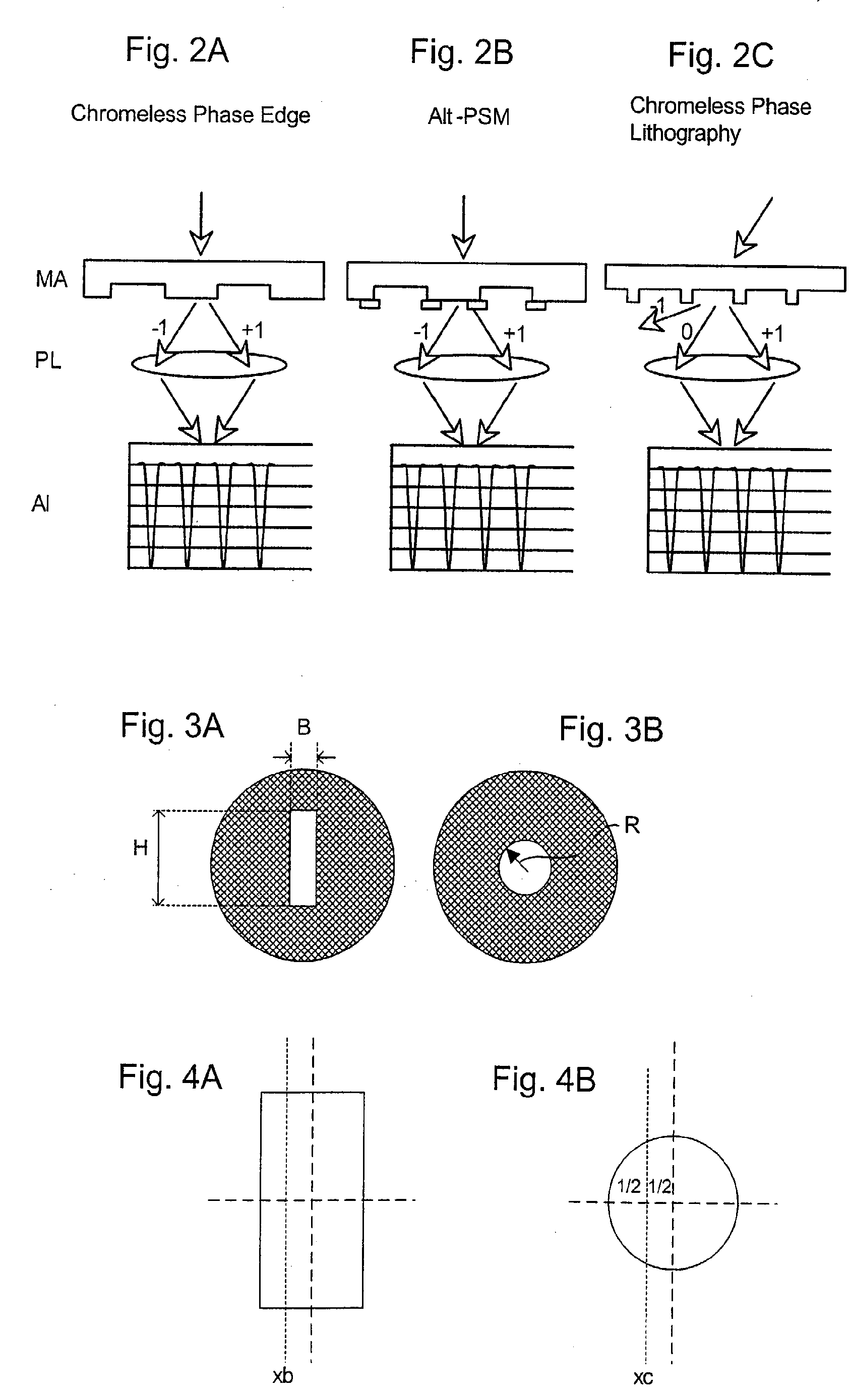
[0076] A second embodiment is the same as the first embodiment except that it uses a cross-shaped on-axis monopole illumination mode, as shown in FIG. 7. A cross-shaped illumination mode has lower average σ value than a circular monopole of equivalent area, or conversely larger area for a given average σ. The cross also has better depth of focus and avoids catastrophic defocus failure as can occur with circular monopoles. Furthermore, the cross is applicable for patterns including gates oriented in two orthogonal directions. The radiation in each arm of the cross is preferably polarized parallel to the elongate direction of the arm, as indicated by arrows in the cross.
[0077] The cross-shaped illumination mode is preferably symmetric about two axes and thence can be characterized by two parameters—the arm width A and the length L. Appropriate values for A and L can be determined in the same way as B and H are determined in the first embodiment. Preferably, the horizontal arm (bar) d...
embodiment 3
[0078] A third embodiment is the same as the first embodiment except that it uses a diamond-shaped (rhomboid) on-axis monopole illumination mode, as shown in FIG. 8. A diamond shape with diameter D has a greater area but the same average σ as a cross with L=D. Hence the diamond has greater efficiency, allowing more rapid exposures (i.e., greater throughput) and less local lens heating.
PUM
| Property | Measurement | Unit |
|---|---|---|
| aspect ratio | aaaaa | aaaaa |
| wavelength | aaaaa | aaaaa |
| wavelength | aaaaa | aaaaa |
Abstract
Description
Claims
Application Information