Systems and Methods for Integrated Antennae Structures in Multilayer Organic-Based Printed Circuit Devices

a printed circuit device and organic-based technology, applied in the direction of radiating element structural forms, resonant antennas, protective material radiating elements, etc., can solve the problems of difficult placement of antennas in an environment free of other conductors, affecting the size, shape and location of antennas, and reducing the space available for additional functions

Active Publication Date: 2008-02-14
KYOCERA AVX COMPONENTS CORP
View PDF99 Cites 62 Cited by
  • Summary
  • Abstract
  • Description
  • Claims
  • Application Information

AI Technical Summary

Benefits of technology

[0008]According to an embodiment of the invention, there is a system for an organic antenna structure. The system may include a first organic layer having a first portion and a second portion, the first portion including a first conductive layer that is patterned to form at least one passive device and a second portion including a second conductive layer that is patterned to form one or more interconnect traces, where the...

Problems solved by technology

There are at least three major challenges for antenna design associated with wireless integration into portable handheld, mobile and laptop applications.
First, many of these applications are very densely packed electronic devices, and leave very little room for additional functions.
Second, FCC emission requirements have forced laptop manufacturers and other portable electronics suppliers to make extensive use of conducting materials in the covers of the laptops or conducting shields to minimize radiation from today's very high-speed processors.
Thus, it is difficult to place an antenna in an environment free enough of other conductors to create an efficient radiator.
Third, the size, shape, and location of the antenna may ...

Method used


Image

  • Systems and Methods for Integrated Antennae Structures in Multilayer Organic-Based Printed Circuit Devices
  • Systems and Methods for Integrated Antennae Structures in Multilayer Organic-Based Printed Circuit Devices
  • Systems and Methods for Integrated Antennae Structures in Multilayer Organic-Based Printed Circuit Devices

Examples


Embodiment Construction

[0026]The present inventions now will be described more fully hereinafter with reference to the accompanying drawings, in which some, but not all embodiments of the invention are shown. Indeed, these inventions may be embodied in many different forms and should not be construed as limited to the embodiments set forth herein; rather, these embodiments are provided so that this disclosure will satisfy applicable legal requirements. Like numbers refer to like elements throughout.

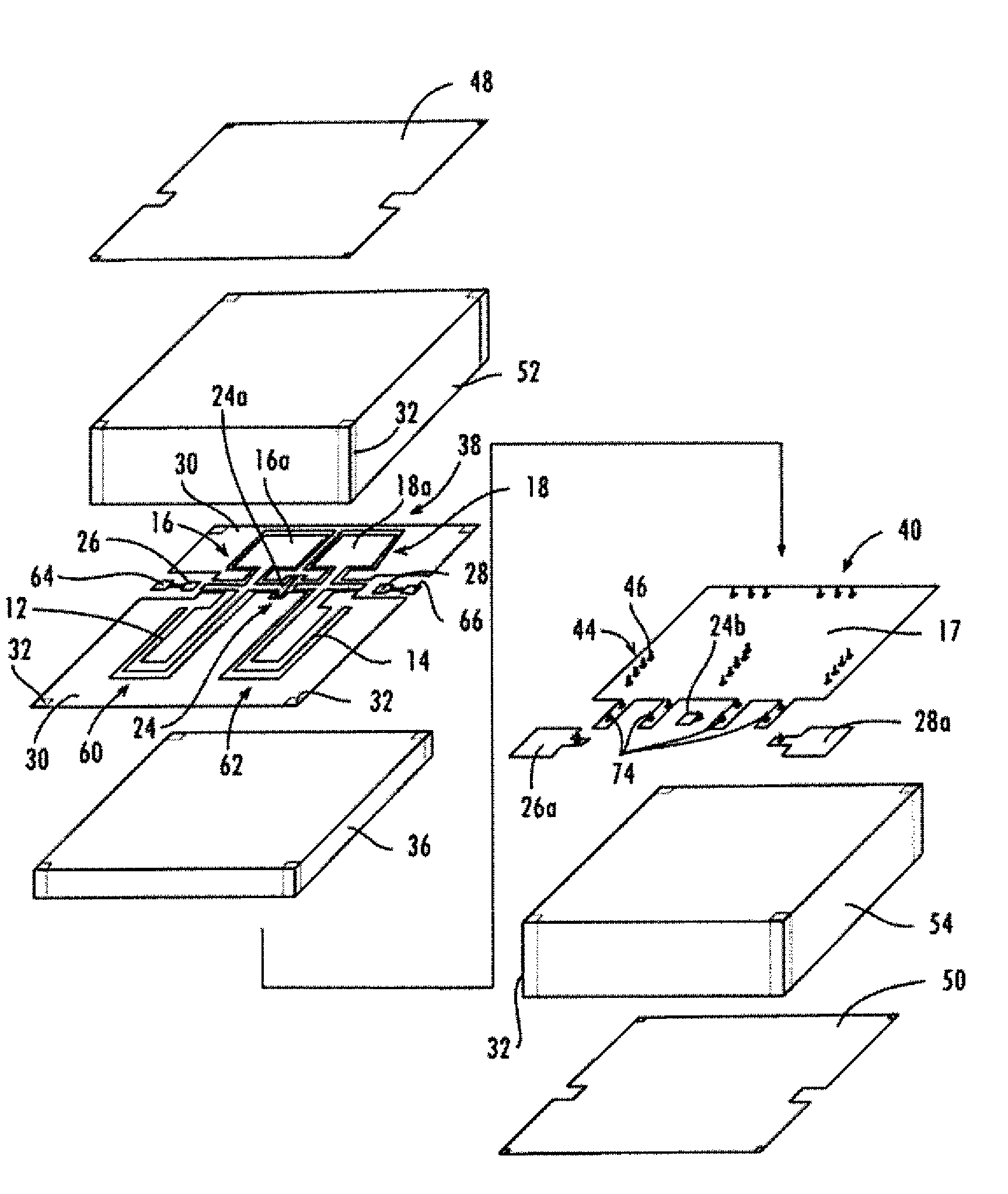
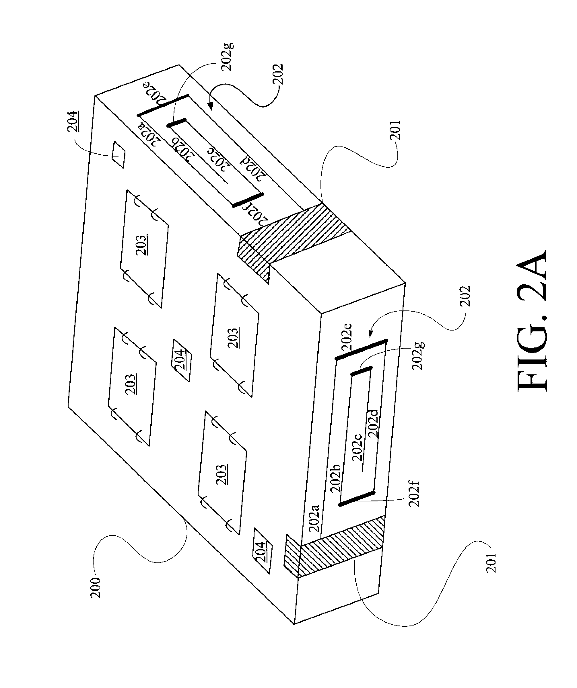
[0027]Embodiments of the present invention may provide for antennae structures that may be formed as a part of a multilayer organic stackup or otherwise connected to a multilayer organic stackup. According to an embodiment of the invention, the antennae structures described herein may be either fabricated as a part of or otherwise connected to integrated organic substrates or integrated passive devices (IPDs), as described in U.S. Pat. Nos. 6,900,708, and 7,068,124 and U.S. patent application Ser. Nos. 10 / 402,3...


PUM


Abstract

Embodiments of the invention may provide for a variety of antennae structures, including the following: a) antennae structures printed directly on the sides of the radio frequency (RF) module or integrated passive device (IPD), b) printed antennae structures fabricated on preformed dielectric lids or overmolds, c) antennae structures fabricated as part of the dielectric wiring that constitutes the wireless module, d) antennae structures that are printed directly on the top of the finished RF module, and e) antennae structures printed directly on the dielectric layers adjacent to thin film wiring and embedded passive elements such as filters, diplexers and couplers.

Description

RELATED APPLICATIONS[0001]This application claims benefit of U.S. Provisional Application No. 60 / 821,888, filed Aug. 9, 2006, an entitled “Systems and Methods for Integrated Antennae Structures in Multilayer Organic-Based Printed Circuit Devices. The application is also related to U.S. Pat. No. 6,900,708, filed on Mar. 28, 2003 as application Ser. No. 10 / 402,315, and entitled “Integrated Passive Devices Fabricated Utilizing Multilayer Organic Laminates;” U.S. Pat. No. 7,068,124, filed on May 27, 2005 as application Ser. No. 11 / 140,630, and entitled “Integrated Passive Devices Fabricated Utilizing Multilayer Organic Laminates;” U.S. application Ser. No. 10 / 402,315, filed on Mar. 28, 2003, and entitled “Methods for fabricating three-dimensional all organic interconnect structures;” and application Ser. No. 11 / 177,508, filed Jul. 8, 2005, and entitled “Heterogeneous Organic Laminate Stack Ups for High Frequency Applications.” All of the foregoing applications are incorporated by refere...

Claims


Application Information

Patent Timeline
IPC IPC(8): H01Q1/38H01Q1/40H01Q9/00
CPCH01Q1/20H01Q1/38H01Q1/243H01Q1/2283H01L2924/181H01L2224/48091H01L2224/48227H01L2924/19105H01L2924/00012H01L2924/00014
Inventor WHITE, GEORGE E.DALMIA, SIDHARTH
Owner KYOCERA AVX COMPONENTS CORP
Why Eureka
Try Eureka