

Imaging device
a technology of a gate electrode and an imager, which is applied in the direction of radiation controlled devices, counting chain synchronous pulse counters, pulse techniques, etc., can solve the problems of disadvantageous data read and data potential change of the electron transfer region corresponding to the gate electrode for reading data
- Summary
- Abstract
- Description
- Claims
- Application Information
AI Technical Summary
Problems solved by technology
Method used
Image

Examples
first embodiment
[0031]A structure of a CMOS image sensor according to a first embodiment will be now described with reference to FIGS. 1 to 5. In the first embodiment, the present invention is applied to a passive CMOS image sensor, which is an exemplary imaging device.
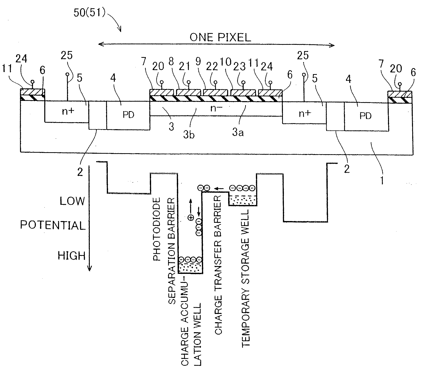
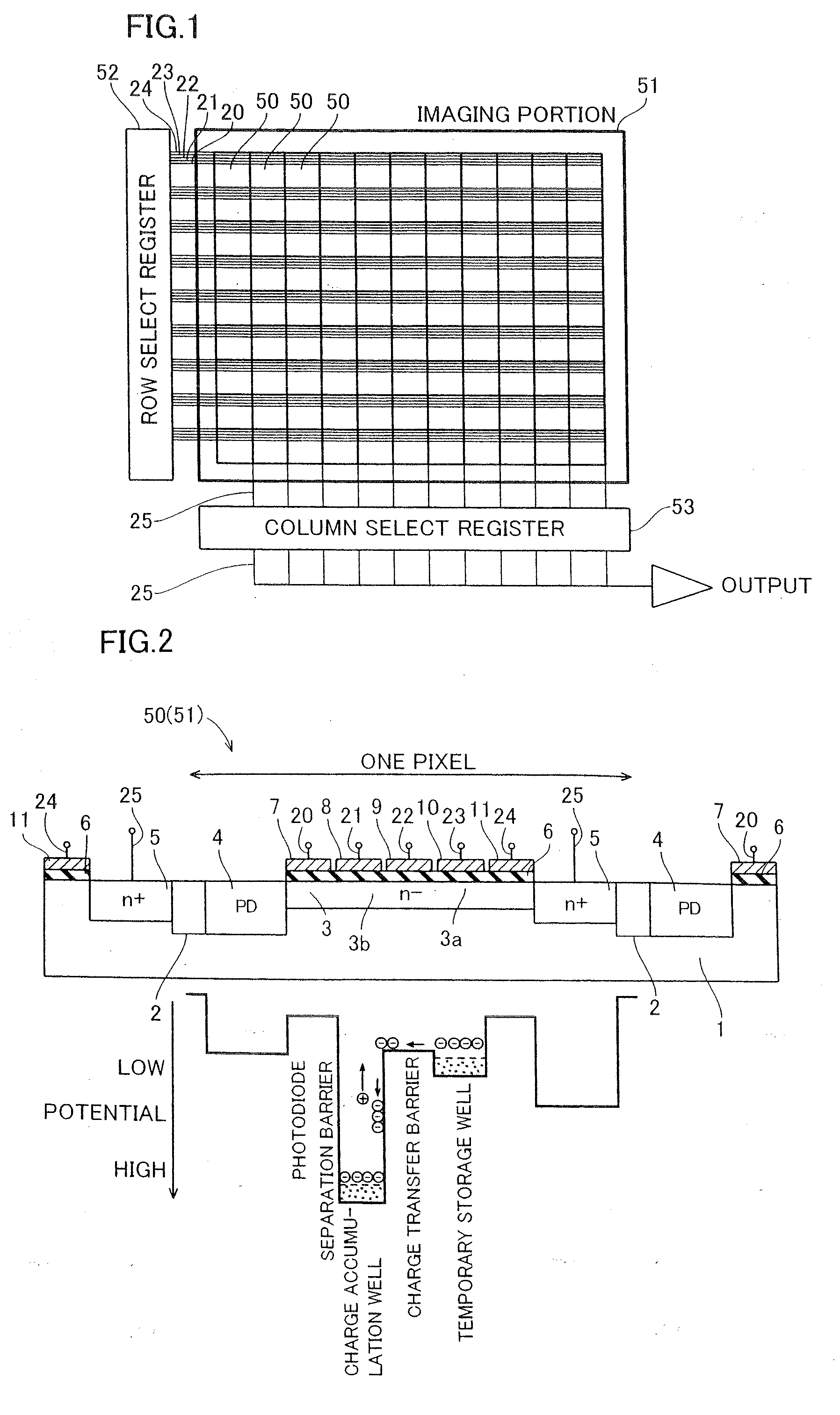
[0032]The CMOS image sensor according to the first embodiment comprises an imaging portion 51 including a plurality of pixels 50 arranged in the form of matrix, a row select register 52 and a column select register 53 as shown in FIG. 1.
[0033]As shown in FIGS. 2 and 3, in a cross-sectional structure of the pixels 50 of the CMOS image sensor according to the first embodiment, element separation regions 2 are formed on a surface of a p-type silicon substrate 1 for separating the pixels 50 respectively. A photodiode portion (PD) 4 and a floating diffusion region 5 consisting of an n+-type impurity region is so formed on a surface of a p-type silicon substrate 1 of each pixel 50 surrounded by the element separation regions 2 as to hold a...
second embodiment
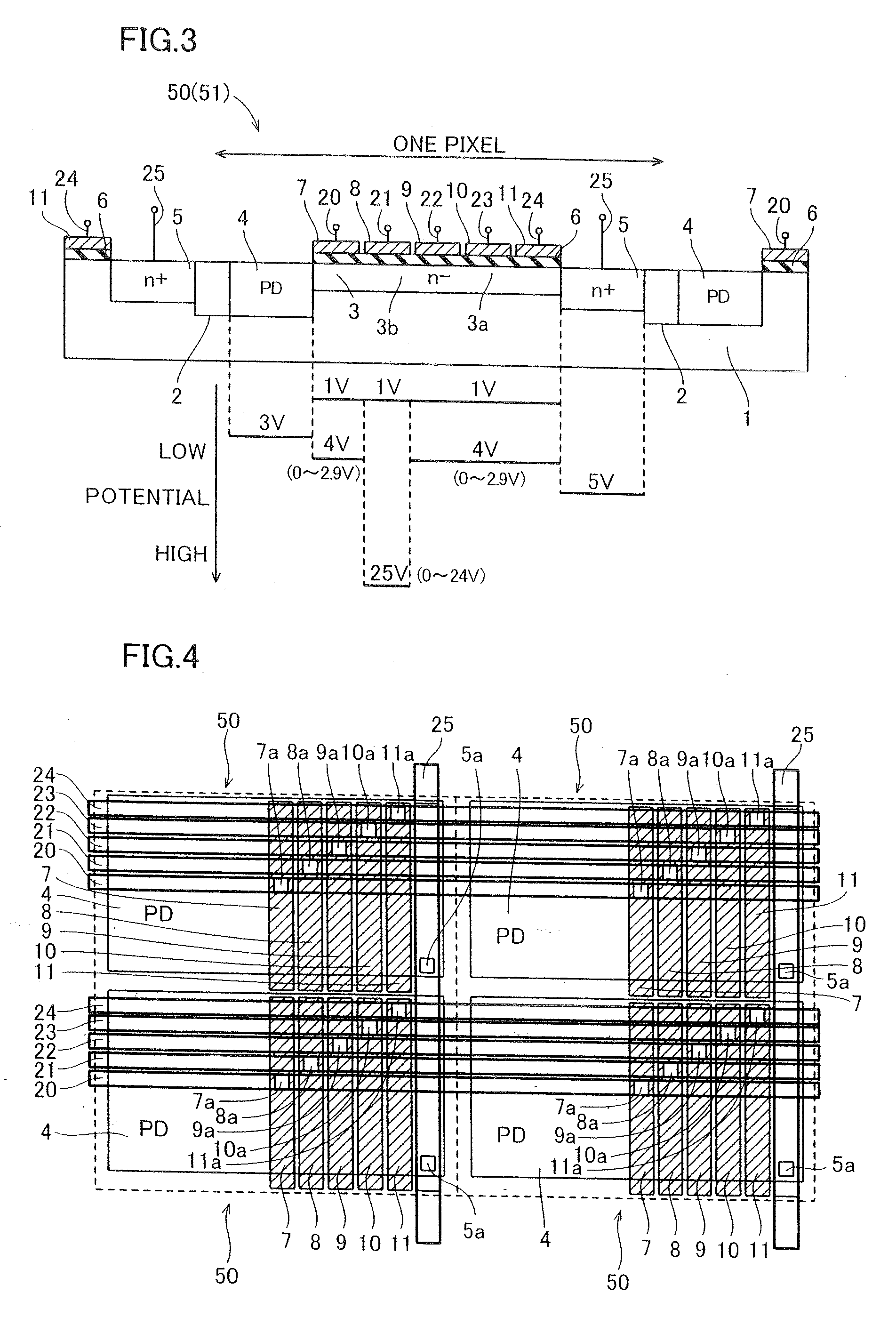
[0063]According to a second embodiment, the potentials of transfer channels 3 located under transfer gate electrodes 7 and readout gate electrodes 11 are adjusted to a potential (higher potential barrier) lower than the potentials of transfer channels 3 under multiplication gate electrodes 8, transfer gate electrodes 9 and transfer gate electrodes 10 when OFF signals (low-level signals) of clock signals Φ1 and Φ5 are supplied to the transfer gate electrodes 7 and the readout gate electrodes 11 dissimilarly to the aforementioned first embodiment.
[0064]According to the second embodiment, when OFF signals (low-level signals) of clock signals Φ2, Φ3 and Φ4 are supplied to the multiplication gate electrodes 8, the transfer gate electrodes 9 and the transfer gate electrodes 10 through wiring layers 21, 22 and 23 respectively, a voltage of about 0 V is applied to the multiplication gate electrodes 8, the transfer gate electrodes 9 and the transfer gate electrodes 10, as shown in FIG. 10. A...
third embodiment
[0079]According to a third embodiment, when OFF signals (low-level signals) of clock signals Φ1 and Φ5 are supplied to transfer gate electrodes 7 and readout gate electrodes 11, the potentials of transfer channels 3 located under the transfer gate electrodes 7 and the readout gate electrodes 11 are adjusted to different potentials (higher potential barriers) lower than the transfer channels 3 located under the potentials of multiplication gate electrodes 8, transfer gate electrodes 9 and transfer gate electrodes 10 dissimilarly to the aforementioned second embodiment.
[0080]According to the third embodiment, when OFF signals (low-level signals) of clock signals Φ2, Φ3 and Φ4 are supplied to the multiplication gate electrodes 8, the transfer gate electrodes 9 and the transfer gate electrodes 10 through wiring layers 21, 22 and 23 respectively, a voltage of about 0 V is applied to the multiplication gate electrodes 8, the transfer gate electrodes 9 and the transfer gate electrodes 10, ...
PUM
 Abstract
Description
Claims
Application Information