Hetrojunction bipolar transistor (HBT) with periodic multilayer base

a bipolar transistor and heterojunction technology, applied in the direction of basic electric elements, electrical equipment, semiconductor devices, etc., can solve the problem of increasing the difficulty of maintaining an fsub>max/sub>/fsub>t /sub>ratio greater than 1.0

a bipolar transistor and heterojunction technology, applied in the direction of basic electric elements, electrical equipment, semiconductor devices, etc., can solve the problem of increasing the difficulty of maintaining an fsub>max/sub>/fsub>t /sub>ratio greater than 1.0

US20080050883A1Inactive Publication Date: 2008-02-28ATMEL CORP

Image

  • Hetrojunction bipolar transistor (HBT) with periodic multilayer base
  • Hetrojunction bipolar transistor (HBT) with periodic multilayer base
  • Hetrojunction bipolar transistor (HBT) with periodic multilayer base

Examples


Embodiment Construction

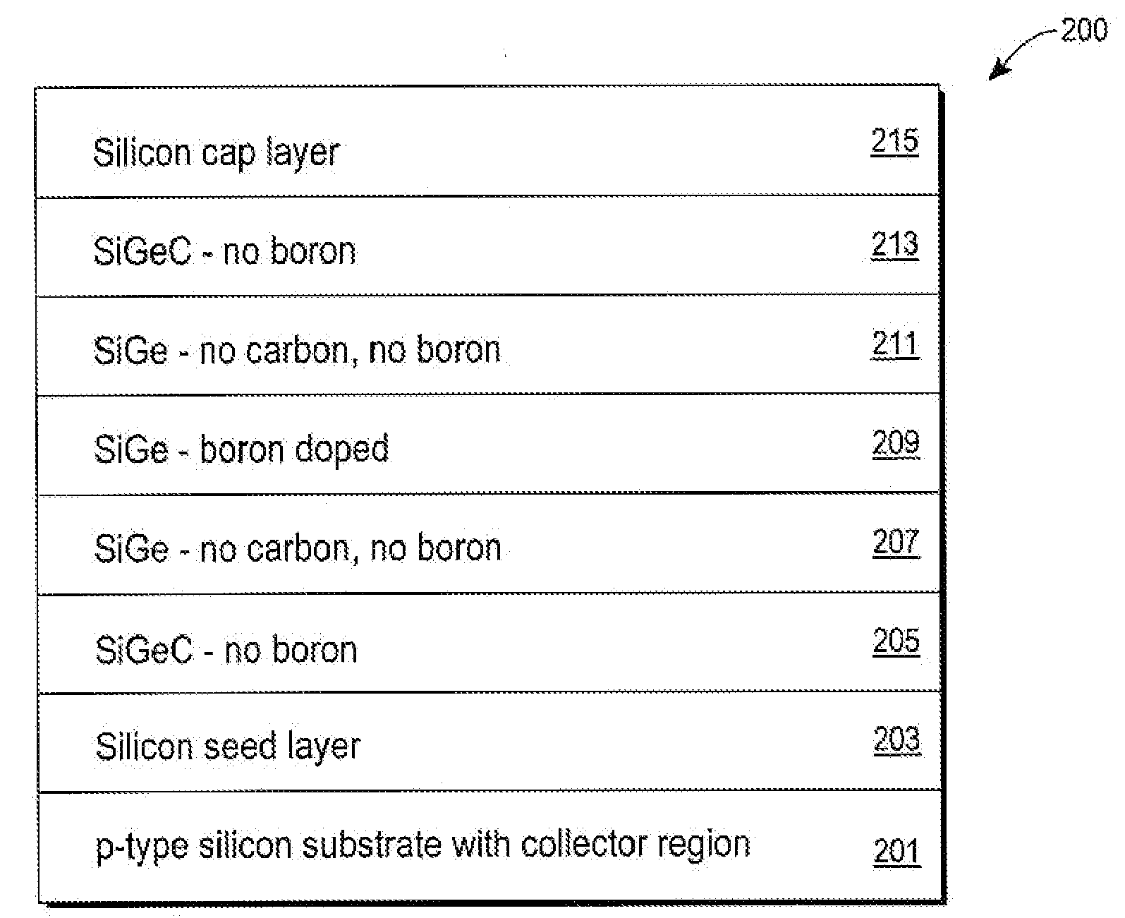
[0030]Critical shortcomings in the prior art exist that must be overcome to realize further benefits of the advantages of SiGe HBTs. The following disclosure relates specifically to an npn-type SiGe HBT, but the principles involved also relates to pnp-type SiGe HBTs as well as HBTs made with other compound semiconductor materials (e.g., other Group III-V or II-VI materials). Additionally, technology and methods disclosed herein benefits other devices types such as, for example, metal oxide semiconductor field effect transistors (MOSFETs), high electron mobility transistors (HEMTs), high hole mobility transistors (HHMTs), bipolar junction transistors (BJTs), and FINFETs.

[0031]The periodic multi-layer (ML) and / or superlattice (SL) have been known for other applications for some time. However, the use of an ML in the base of a SiGe HBT represents a new utilization of this technology. The SL is a special case of an ML, in which layers that are chemically different from adjacent neighbor...


PUM


Abstract

A method and resulting electronic device utilizing a periodic multi-layer (ML) and/or superlattice (SL) structures in the base of a SiGe heterojunction bipolar transistor (HBT) is disclosed. The SL is a special case of an ML, in which layers that are chemically different from adjacent neighbors are successively repeated. The use of the ML in electronic and photonic devices is enables strategic engineering of the energy band gap and carrier mobilities. Principles disclosed herein relate to npn- and pnp-type SiGe HBTs as well as HBTs made with other compound semiconductor materials (e.g., other Group III-V or II-VI materials). Additionally, technology and methods disclosed herein benefit other devices types such as, for example, metal oxide semiconductor field effect transistors (MOSFETs), high electron mobility transistors (HEMTs), high hole mobility transistors (HHMTs), bipolar junction transistors (BJTs), and FINFETs.

Description


Claims


Application Information

Patent Timeline
28 Feb 2008
Publication
US20080050883A1