Polarized light emitting diode and method of forming the same

a light-emitting diode and polarized technology, applied in the direction of semiconductor/solid-state device manufacturing, electrical apparatus, semiconductor/semiconductor devices, etc., can solve the problem of relatively low light-emitting efficiency

Inactive Publication Date: 2008-03-06
SAMSUNG ELECTRONICS CO LTD
View PDF13 Cites 36 Cited by
  • Summary
  • Abstract
  • Description
  • Claims
  • Application Information

AI Technical Summary

Benefits of technology

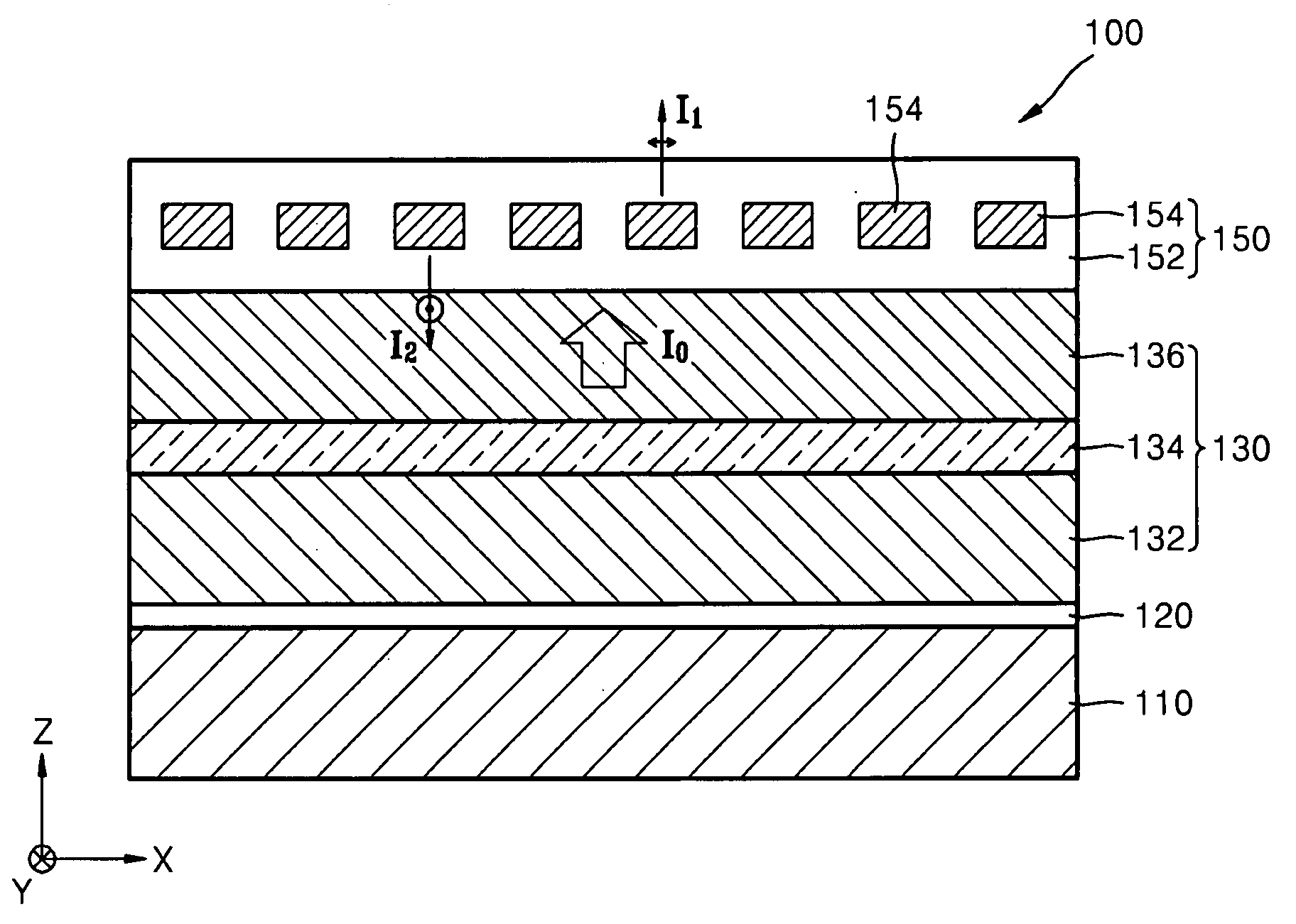
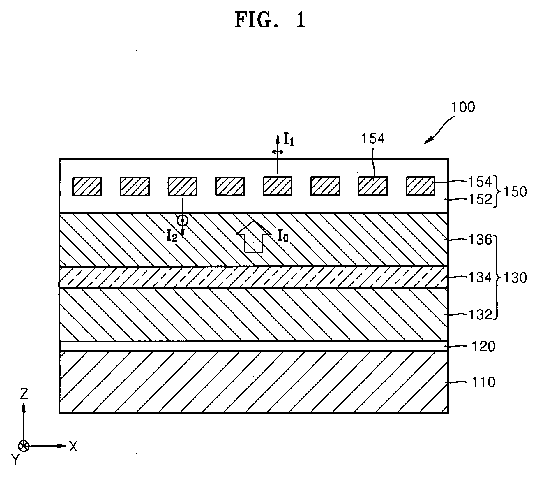
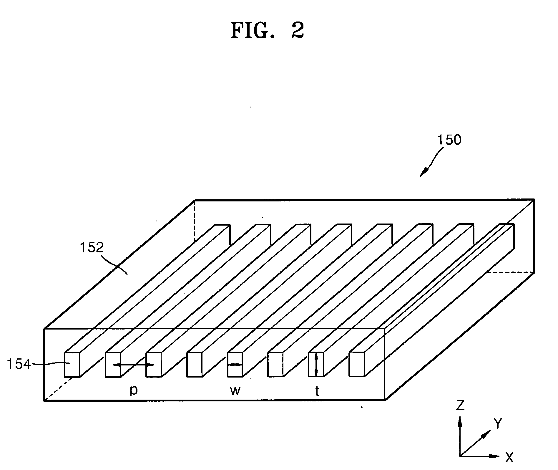
[0007]The polarization control layer may include a dielectric layer in which the metal nanowires may be formed. The metal nanowires may have a polygonal cross-section or circular cross-section, including, for example, a rectangular cross-section. The plurality of metal nanowires may have a thickness ranging from about 50 nm to about 1000 nm inclusive. The metal nanowires may have a width less than or equal to about half the pitch of the plurality of parallel metal nanowires.
[0008]According to example embodiments, the polarized light emitting diode may also include a reflecting layer arranged between the support layer and the semiconductor layer structure. The plurality of metal nanowires may have a pitch less than or equal to about half of the wavelength of light emitted from the light-emitting layer. The metal nanowires may be formed of for example Al, Au, Ag, Pd, Pt, an alloy thereof or the like. The plurality of metal nanowires may be used as electrodes to apply a voltage to the semiconductor layer structure.
[0009]According to example embodiments, the polarized light emitting diode may also include a depolarizing layer for depolarizing light reflected from the polarization control layer. The depolarizing layer may be formed of an optical anisotropic material having a refractive variable index. The reactive index may vary with the polarization of incident light, and may be a scattering layer.
[0010]The depolarizing layer may be arranged between the polarization control layer and the semiconductor layer structure, within the semiconductor layer structure, or between the support layer and the semiconductor layer structure. If a reflecting layer is formed between the support layer and the semiconductor layer structure, the depolarizing layer may be formed between the reflecting layer and the semiconductor layer structure as well.
[0011]Example embodiments may further include a reflecting layer formed on side surfaces of the support layer, the semiconductor layer structure, and / or the polarization control layer.
[0012]According to example embodiments, a method of forming a polarized light emitting diode may include forming a semiconductor layer structure on a substrate. The semiconductor layer structure may include a first semiconductor layer, a light emitting layer, and a second semiconductor layer. A reflecting layer may be formed on the second semiconductor layer, and a support layer may be formed and attached to the reflecting layer. The substrate may be removed from the semiconductor layer structure, and the polarization control layer may be formed on the first semiconductor layer. The polarization control layer may include metal nanowires.

Problems solved by technology

Because the polarization plates may absorb about 50 percent of incident light, light efficiency may be relatively low.

Method used


Image

  • Polarized light emitting diode and method of forming the same
  • Polarized light emitting diode and method of forming the same
  • Polarized light emitting diode and method of forming the same

Examples


Embodiment Construction

[0021]Detailed example embodiments are disclosed herein. However, specific structural and functional details disclosed herein are merely representative for purposes of describing example embodiments. Example embodiments may, however, be embodied in many alternate forms and should not be construed as limited to only the embodiments set forth herein.

[0022]Accordingly, while example embodiments are capable of various modifications and alternative forms, embodiments thereof are shown by way of example in the drawings and will herein be described in detail. It should be understood, however, that there is no intent to limit example embodiments to the particular forms disclosed, but to the contrary, example embodiments are to cover all modifications, equivalents, and alternatives falling within the scope of example embodiments. Like numbers refer to like elements throughout the description of the figures.

[0023]It will be understood that, although the terms first, second, etc. may be used h...


PUM


Abstract

Example embodiments are directed to a polarized light emitting diode and method of forming the same. The polarized light emitting diode may include a support layer, a semiconductor layer structure, and/or a polarization control layer. The semiconductor layer structure may be formed on the support layer and may include a light-emitting layer. The polarization control layer may be formed on the semiconductor layer structure and may include a plurality of metal nanowires. The polarized light emitting diode may be configured to control the polarization of emitted light. The method of forming a polarized light emitting diode may include forming on a substrate a semiconductor layer structure with a light emitting layer. A reflecting layer may be formed on the semiconductor layer structure with an attached support layer. The substrate may be removed from the semiconductor layer structure and a polarization control layer including metal nanowires may be formed on the semiconductor layer structure.

Description

PRIORITY STATEMENT[0001]This application claims the benefit of Korean Patent Application No. 10-2006-0082935, filed on Aug. 30, 2006, in the Korean Intellectual Property Office, the disclosure of which is incorporated herein in its entirety by reference.BACKGROUNDDescription of the Related Art[0002]Recently, light emitting diodes have gained attention as a new, increasingly efficient, environmental light source. They have been used in a wide range of applications, including, for example, vehicle light sources, display device light sources, optical communications and general lighting sources.[0003]In a variety of applications, polarization properties of light may be used to take advantage of light emitted from a source. A liquid crystal display device may be formed by injecting a liquid crystal material between substrates on which electrodes may be formed. When a voltage is applied between the two electrodes, an electrical field may be generated to change the liquid crystal molecular...

Claims


Application Information

Patent Timeline
Patent Type & Authority Applications(United States)
IPC IPC(8): H01L33/00H01L33/06H01L33/10H01L33/32
CPCH01L33/44
Inventor MIN, BOK-KISONE, CHEOL-SOO
Owner SAMSUNG ELECTRONICS CO LTD
Why Eureka
Try Eureka