SRAM static noise margin test structure suitable for on chip parametric measurements

a static noise margin and test structure technology, applied in static storage, information storage, digital storage, etc., can solve the problems of sram bit easily being upset, time consumed in memory cell testing can become a significant issue, and test designs are designed to be extensive and exhaustive. , to achieve the effect of fast on-chip assessment of snm

a static noise margin and test structure technology, applied in static storage, information storage, digital storage, etc., can solve the problems of sram bit easily being upset, time consumed in memory cell testing can become a significant issue, and test designs are designed to be extensive and exhaustive. , to achieve the effect of fast on-chip assessment of snm

US20080062746A1Active Publication Date: 2008-03-13TEXAS INSTR INC

Image

  • SRAM static noise margin test structure suitable for on chip parametric measurements
  • SRAM static noise margin test structure suitable for on chip parametric measurements
  • SRAM static noise margin test structure suitable for on chip parametric measurements

Examples


Embodiment Construction

[0059]One or more aspects of the present invention are described with reference to the drawings, wherein like reference numerals are generally utilized to refer to like elements throughout, and wherein the various structures are not necessarily drawn to scale. In the following description, for purposes of explanation, numerous specific details are set forth in order to provide a thorough understanding of one or more aspects of the present invention. It may be evident, however, to one skilled in the art that one or more aspects of the present invention may be practiced with a lesser degree of these specific details. In other instances, known structures and devices are shown in block diagram form in order to facilitate describing one or more aspects of the present invention.

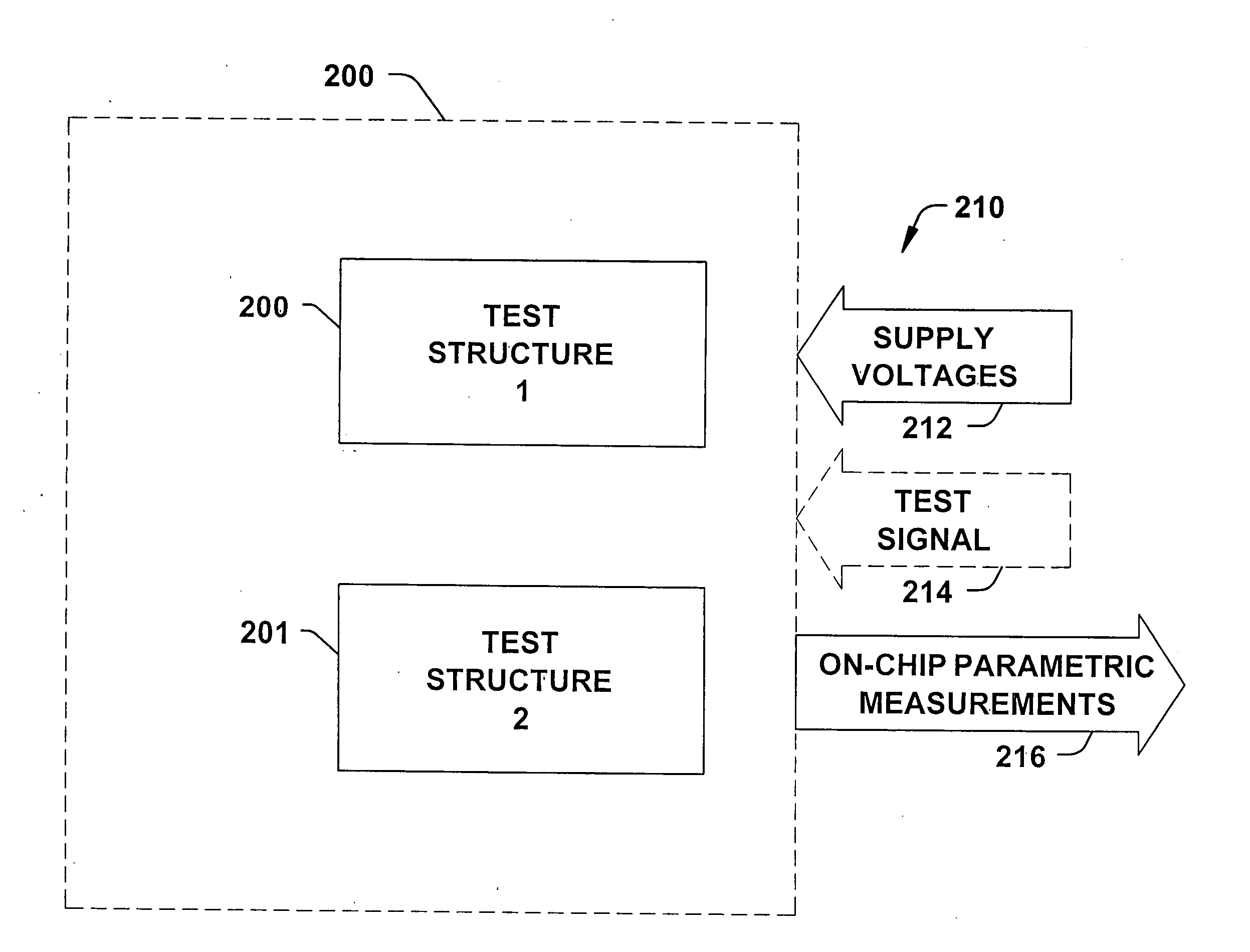
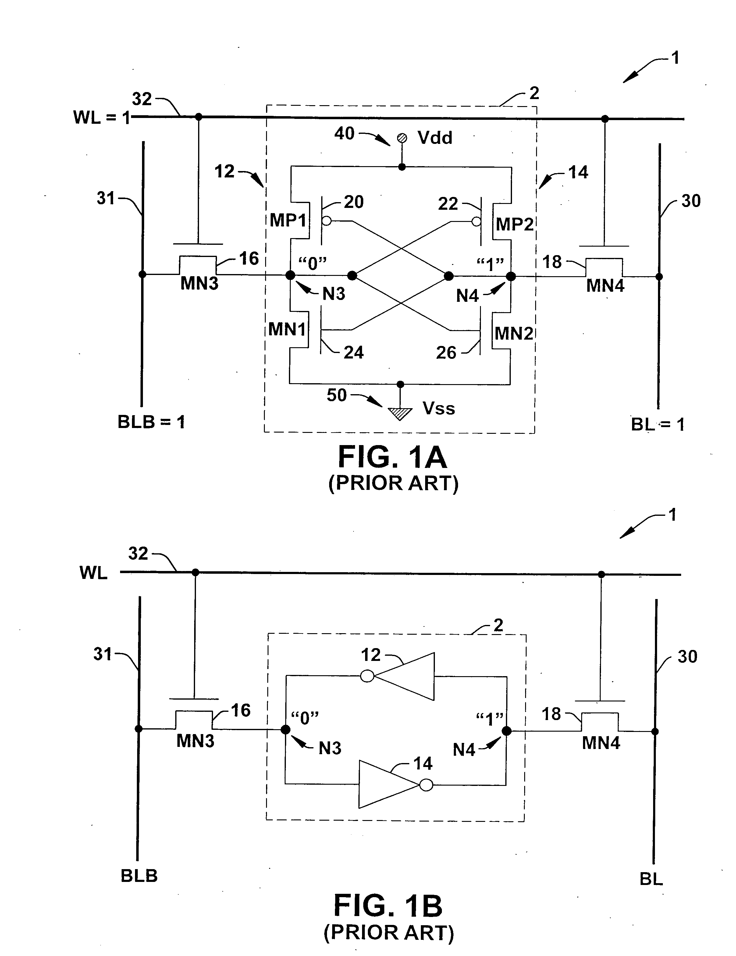
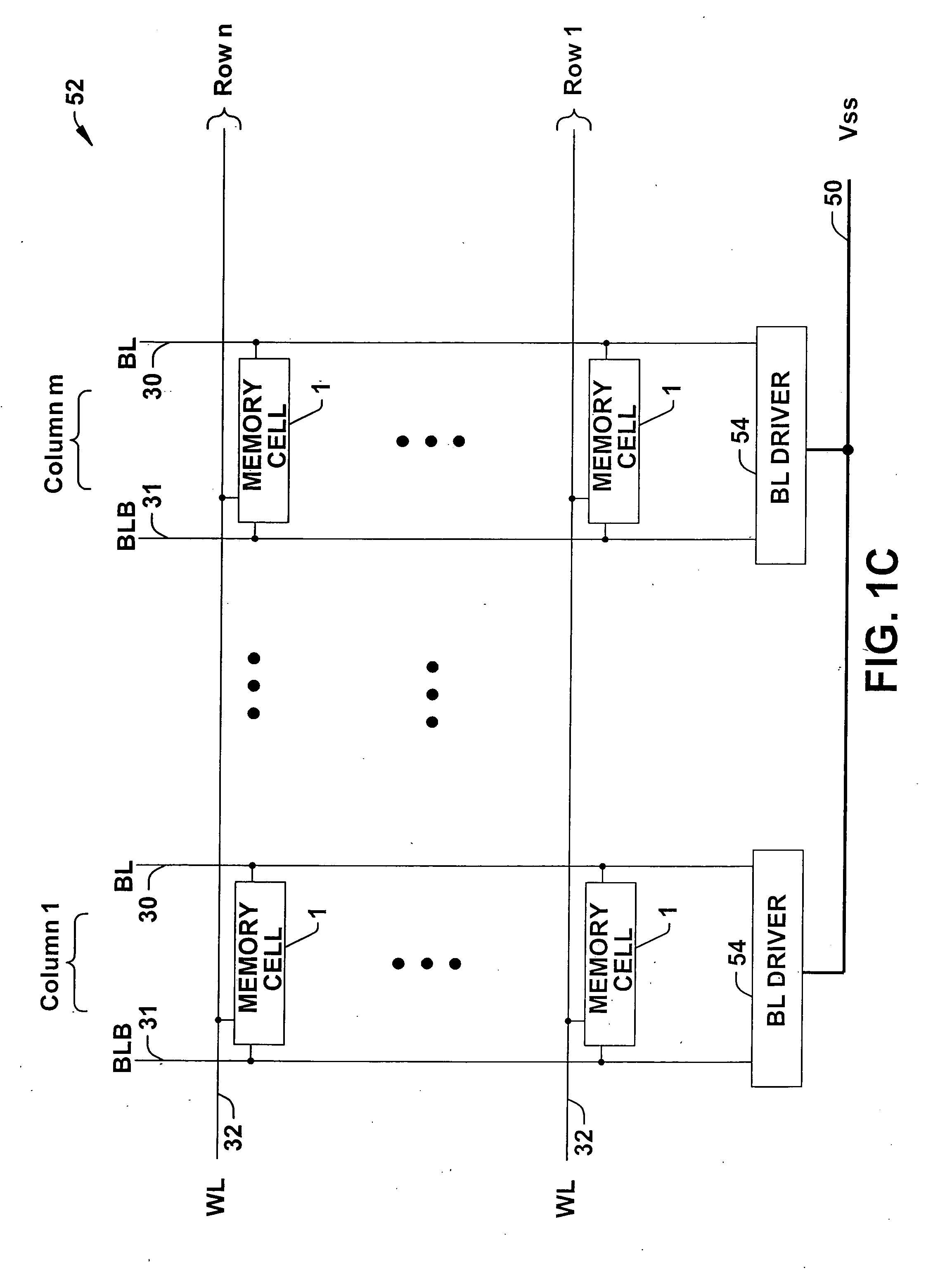
[0060]The present invention pertains to a set of memory test structures and methods for assessing (e.g., on-chip or at wafer level testing) the memory cells of a semiconductor or integrated circuit device, which pr...


PUM


Abstract

A set of memory cell test structures and a method are disclosed for assessment of the static noise margin (SNM) of a memory cell or an array of such cells, for example, of SRAM cells of an integrated circuit device, using discrete point measurement structures provided either on-chip or within the scribe lines. In one embodiment, the set of memory structures comprises first and second test structures, individually comprising a memory cell, having one or more left and right half-bit test structures having hard-wired connections between select nodes of each memory cell half-bit and one or more voltage supplies. The half-bits of the first test structure are configured for measuring respective left and right standby SNM values, and the half-bits of the second test structure are configured for measuring respective left and right cell ratio values at respective output nodes of the structures, using applied supply voltages for on-chip assessment of the static noise margin of the memory cells. The method applies the supply voltages to select nodes of the test structures, measures left and right standby SNM values at a first test structure, measures left and right cell ratio values at a second test structure, determines a first difference between the left half-bit standby SNM value and the right half-bit cell ratio value, determines a second difference between the right half-bit standby SNM value and the left half-bit cell ratio value, and determines a smaller one of the first and second difference values proportional to an SNM value of the cell.

Description

FIELD OF INVENTION[0001]The present invention relates generally to integrated circuit devices, and more particularly to methods and test structures suitable for early and massive on-chip assessment of the static noise margin (SNM) of a static random access memory (SRAM) memory cell or array of such cells of an integrated circuit device without the time consuming acquisition and post processing of voltage transfer “butterfly curves” to derive SNM, but rather by using discrete point measurement structures provided either on-chip or within the scribe lines.BACKGROUND OF THE INVENTION[0002]Memory tests are devised to uncover faults with storage cells and the access to these storage cells arising in part from improper design, lack of design margins or processing deficiencies. Generally, these tests are designed to be extensive and exhaustive to ensure that no bit defects, either hard defects or intermittent failures find their way into the field.[0003]Semiconductor memories can, for exam...

Claims


Application Information

Patent Timeline
13 Mar 2008
Publication
US20080062746A1
IPC
G11C11/00; G11C7/02; G11C29/00; G11C7/00
CPC
G11C7/02; G11C11/41; G11C29/24; G11C29/50; G11C2029/5002
Inventors
LOH, WAH KIT; REDWINE, DONALD JAMES