Method for detecting the center of wafer and storage medium storing a program for executing the method

a technology of storage medium and center, which is applied in the direction of semiconductor/solid-state device testing/measurement, instruments, material analysis, etc., can solve the problems of reducing the time for aligning the wafer w, and achieve the effect of shortening the wafer alignment time and reducing the moving amount of the mounting tabl

Inactive Publication Date: 2008-03-20
TOKYO ELECTRON LTD
View PDF11 Cites 15 Cited by
  • Summary
  • Abstract
  • Description
  • Claims
  • Application Information

AI Technical Summary

Benefits of technology

[0021]In accordance with the aspects of the present invention, it is possible to provide a method for detecting the center of a wafer, which is capabl

Problems solved by technology

As a consequence, a moving amount of the mounting table 5 increases, and a long period of time is

Method used


Image

  • Method for detecting the center of wafer and storage medium storing a program for executing the method
  • Method for detecting the center of wafer and storage medium storing a program for executing the method
  • Method for detecting the center of wafer and storage medium storing a program for executing the method

Examples


Embodiment Construction

[0030]Hereinafter, embodiments of the present invention will now be described with respect to FIGS. 1 to 5C which form a part hereof.

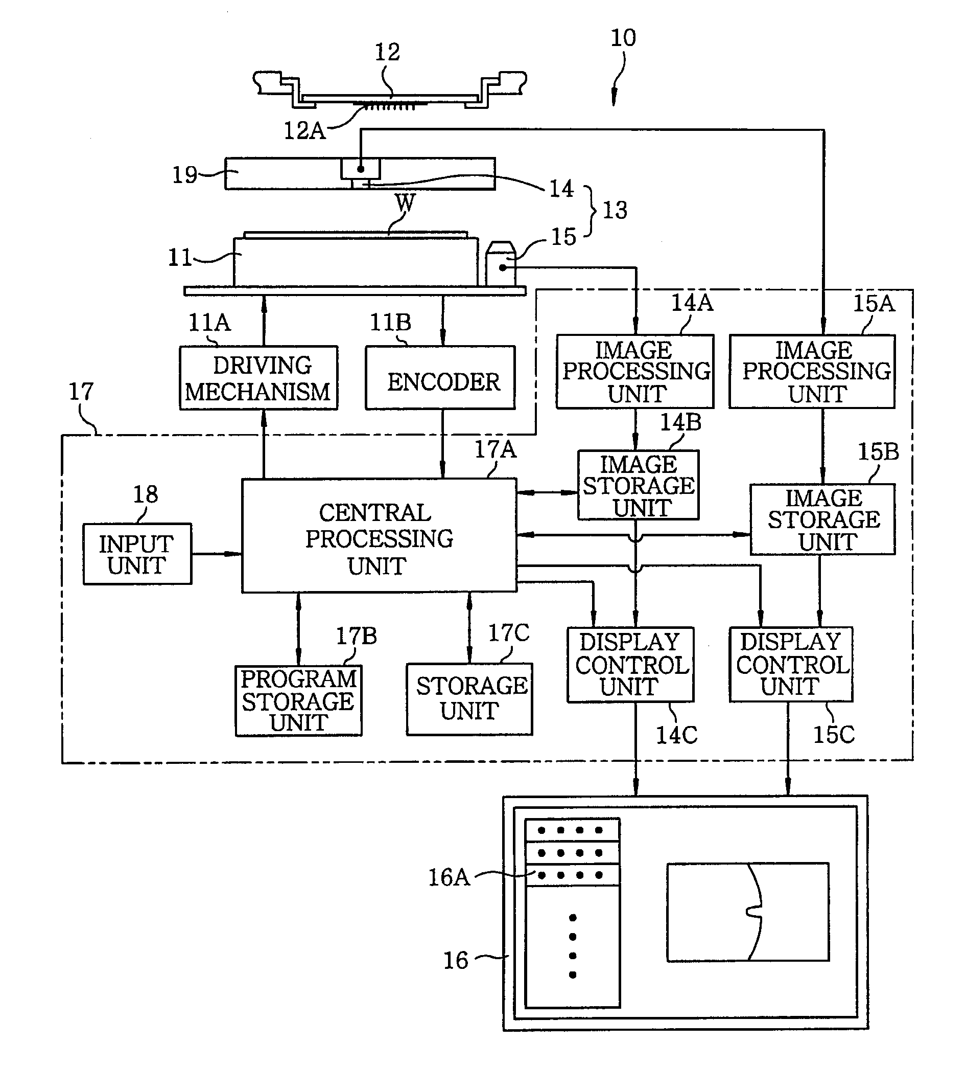
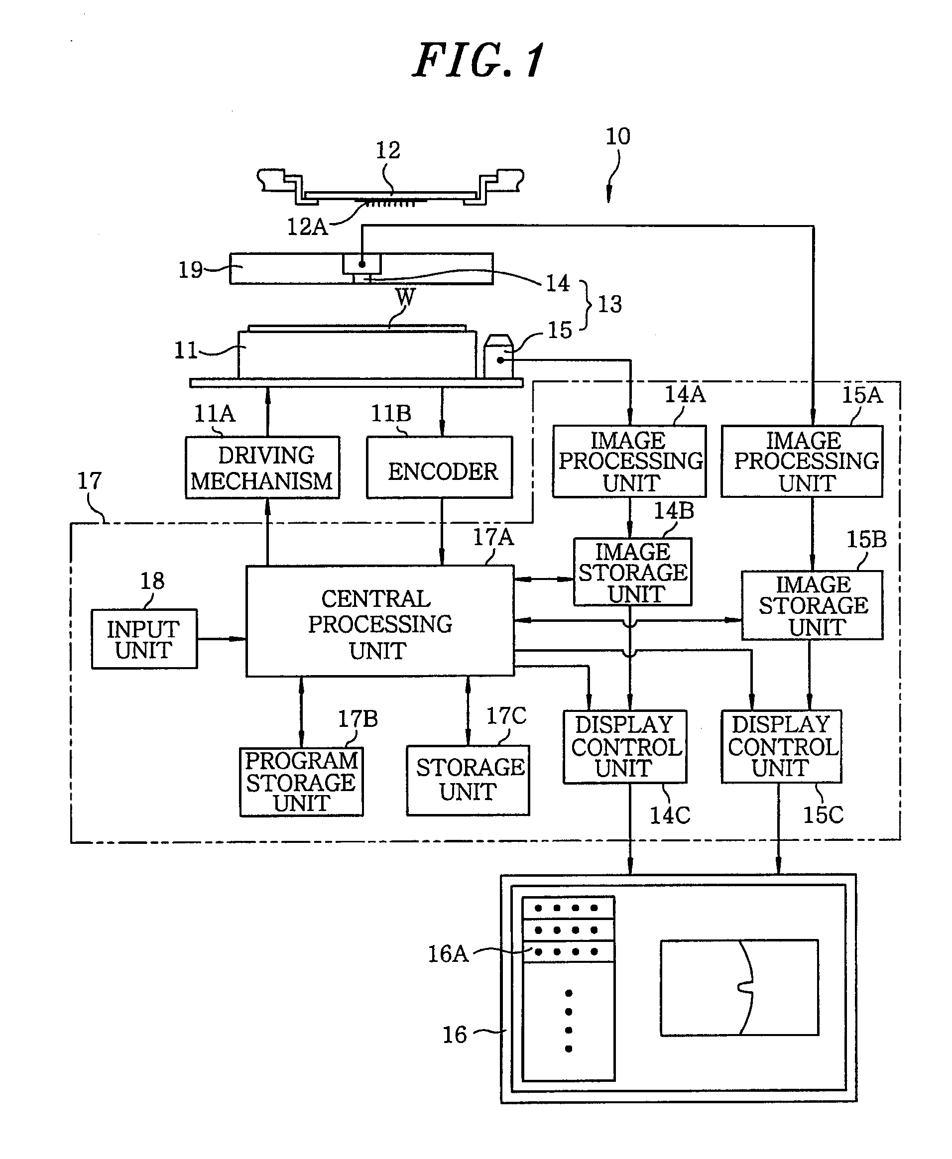
[0031]As illustrated in FIG. 1, an inspection apparatus 10 of an embodiment of the present invention includes a movable mounting table 11 for mounting thereon a wafer W serving as an object to be inspected and having a notch; a probe card 12 provided above the mounting table 11; an alignment mechanism 13 for performing an alignment between a plurality of probes 12A of the probe card 12 and the wafer W on the mounting table 11; a first and a second imaging units (e.g., a first and a second CCD camera 14 and 15) constituting the alignment mechanism 13; a display unit having a display screen 16 for displaying thereon images captured by the first and the second CCD camera 14 and 15; and a controller 17 formed of a computer for controlling the above described parts. The inspection apparatus is configured to inspect the electrical characteristics of the wafe...


PUM


Abstract

A method detects a center of a wafer having a notch when aligning the wafer mounted on a movable mounting table. The method includes capturing an image of the wafer by using an imaging unit, the image including the notch; extracting an edge line from the image of the wafer; detecting a shape of the notch from the edge line; and calculating the center of the wafer based on the shape of the notch.

Description

FIELD OF THE INVENTION[0001]The present invention relates to a method for detecting the center of a wafer to position or align the wafer before performing various processings on the wafer mounted on a mounting table, and a storage medium storing a program for executing the method.BACKGROUND OF THE INVENTION[0002]A process for manufacturing semiconductor devices from a wafer includes various processing steps, and each of the processing steps is performed on the wafer mounted on a mounting table. An alignment operation for precisely positioning the wafer is often performed prior to a specific processing step to be performed on the wafer.[0003]In case a wafer is inspected by an inspection apparatus shown in FIG. 5 for example, the alignment between a plurality of test electrodes of each device of the wafer and probes corresponding thereto is performed before the inspection is carried out by allowing electrical contact between the test electrodes and the corresponding probes. As illustr...

Claims


Application Information

Patent Timeline
IPC IPC(8): G01B11/14
CPCH01L21/681H01L22/00
Inventor KAGAMI, FUMITO
Owner TOKYO ELECTRON LTD
Why Eureka
Try Eureka