
Surface adapting cap with integral adapting material for single and multi chip module assembly

Inactive Publication Date: 2008-03-27
GLOBALFOUNDRIES INC
View PDF7 Cites 15 Cited by
  • Summary
  • Abstract
  • Description
  • Claims
  • Application Information

AI Technical Summary

Benefits of technology

[0007]To mitigate the aforesaid drawbacks the aim of the present invention is to provide a method and an apparatus to accommodate chip warping, position and angle tolerances for single and multi chip module.
[0008]Another object of the invention is to reduce the gap tolerance between the semiconductor chip and cap and hence to increase the thermal performances by maintaining a constant gap thickness at every chip position and for every chip on the module thus compensating for the tolerances caused by variabilities in the cold plate, chip fabrication and in the controlled collapse chip connection (C4) soldering protocol.

Problems solved by technology

This tolerance is caused by warpage of the chip, as well as position and angular tolerances in the placement of each chip.
This arrangement fails to address the problems arising out of the warpage of the semiconductor chips.
This understructure is not capable of providing enough pressure for a low viscosity medium to adapt to convex and concave chip warpage as it does not seal the deformable structure at the periphery.

Method used


Image

  • Surface adapting cap with integral adapting material for single and multi chip module assembly
  • Surface adapting cap with integral adapting material for single and multi chip module assembly
  • Surface adapting cap with integral adapting material for single and multi chip module assembly

Examples


Embodiment Construction

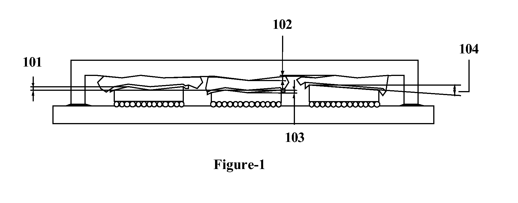
[0030]An embodiment of the present invention provides an adaptive material integral to the cap that adapts to the warping and placement tolerances of the chip. This may be better understood with the aid of the FIG. 1, which shows typical tolerances in multi chip module packing. In this z-offset 101, cap bow 102, chip bow 103, and angle tolerance 104 are shown, where multiple chips are mounted onto a common substrate and covered with a cap. On the bottom side of the cap is a thermally conductive material integrated which adjusts for the non-uniformity between cap and chip and defines a constant and equal gap between chip and cap. This gap then gets filled with a compliant thermal interface material such as paste, gel or adhesive.

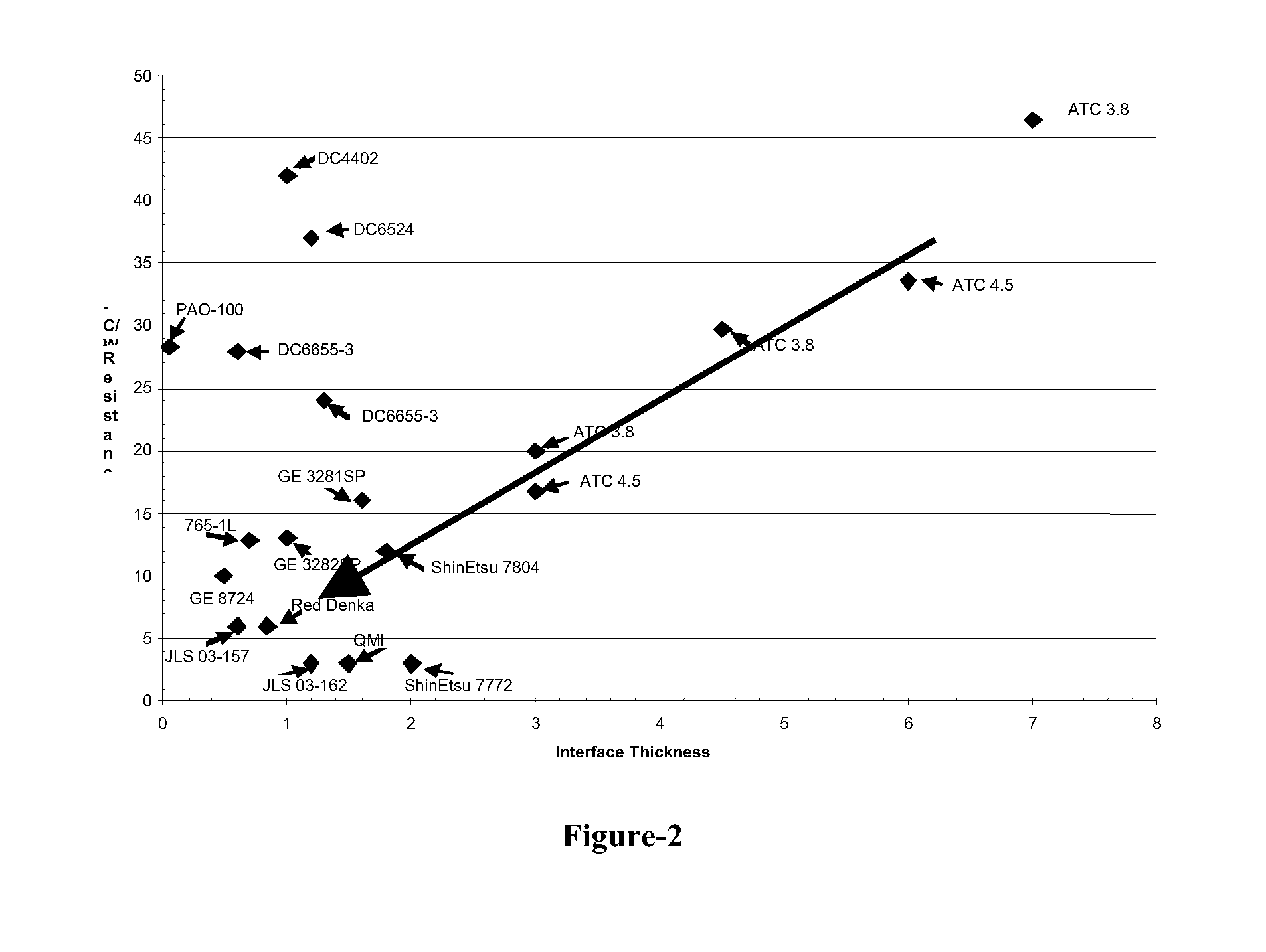
[0031]FIG. 2, illustrates the variation in thermal resistance as a function of interface thickness for different paste materials with the arrow showing the current trend towards smaller and smaller gaps. The ratio between the gap thickness and the thermal res...


PUM


Abstract

A surface adapting cap with an integrated adapting thermally conductive material on single and multi chip module provides reduced gap tolerance and hence better thermal performance of the semiconductor device which enhances the reliability of the semiconductor device. In one of the embodiments the cap is modified with an integrated, confined, and high thermal adaptive material. The membrane on this system is highly flexible. The cap is preassembled to the chip at a temperature above liquidus below curing temperature of the adaptive material. At this state, a hydrostatic pressure in the material develops due to the compression exerted from the cap to the chip and the confined volume of the buried material. This hydrostatic pressure causes the membrane to deflect and to adapt the warping and tolerances of the chip. Due to the adaptive surface the gap on each position of the chip and from chip to chip is same.

Description

FIELD OF INVENTION[0001]The present invention relates to an improved surface adapting cap with an integrated adapting thermally conductive material on one or more semiconductor chips in single and multi chip modules.BACKGROUND OF THE INVENTION[0002]The present invention is related to semiconductor device manufacturing technology, and in particular to the integrated circuit (IC) packaging. Semiconductor device manufacturing technology is continually being pushed to higher levels of density and speed, with the objective of offering ever increasing functionality in a single package. This trend is resulting in sharply increasing power densities that demand continuous improvements in cooling efficiency. The introduction of multichip modules has intensified the need for efficient cooling even further by creating a more complex thermal environment. The Controlled Collapse Chip Connection (C4) protocol has emerged as the dominant assembly process for semiconductor chips in the Single Chip M...

Claims


Application Information

Patent Timeline
IPC IPC(8): H01L23/12
CPCH01L23/433H01L2224/16H01L2224/73253H01L2924/10158H01L2924/16152H01L2924/01322H01L2924/01019H01L2924/00014H01L2924/00011H01L2224/0401
Inventor BRUNSCHWILER, THOMAS JMICHEL, BRUNOLINDERMAN, RYAN JOSEPHKLOTER, URSROTHUIZEN, HUGO E
Owner GLOBALFOUNDRIES INC
Learn More