This helps you quickly interpret patents by identifying the three key elements:
Problems solved by technology
Method used
Benefits of technology
Benefits of technology
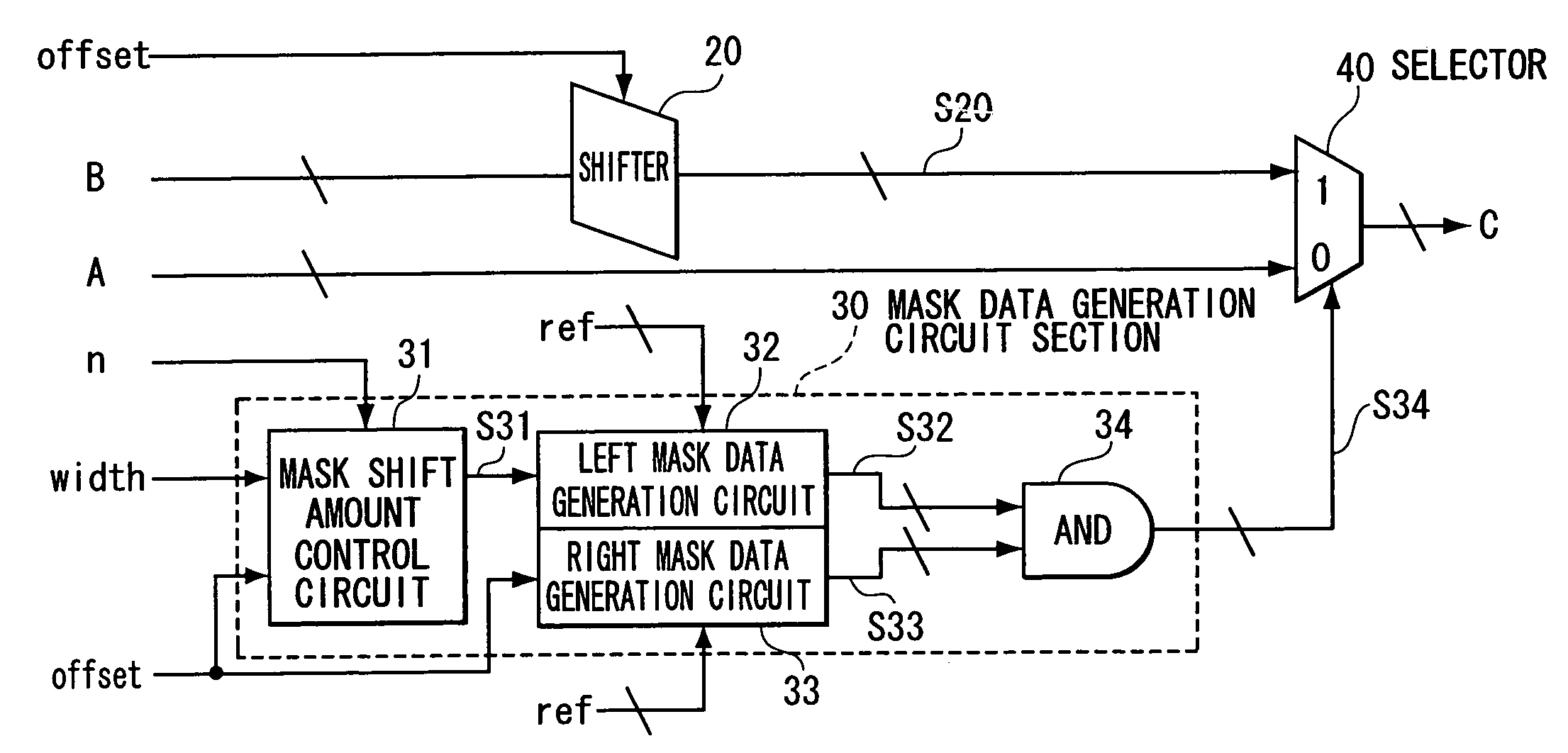
[0022]According to an aspect of the invention, there is provided a bit field operation circuit comprising: a first shift unit that shifts n bits (n being an integer of 2 or more) of first input data in a direction from a least significant bit to a most significant bit based on a first control signal, and generates and outputs n bits of first intermediate data; a mask shift amount control circuit to which the first control signal, a second control signal and a third control signal are input, that determines a mask shift amount on the basis of the first, second and third control signals, and outputs a mask shift control signal in accordance with the mask shift amount; a second shift unit that shifts n bits of reference data in a direction from the most significant bit to the least significant bit based on the mask shift control signal, and generates and outputs n bits of second intermediate data; a third shift unit that shifts the reference data in a direction from the least significant bit to the most significant bit on the basis of the first control signal, and generates and outputs n bits of third intermediate data; a logic operation unit that performs a logical operation on the second intermediate data and the third intermediate data, and generates and outputs n bits of mask selection data; and a selection unit that selects either one of the first intermediate data or n bits of second input data based on the mask selection data so as to output as n bits of output data.
Problems solved by technology
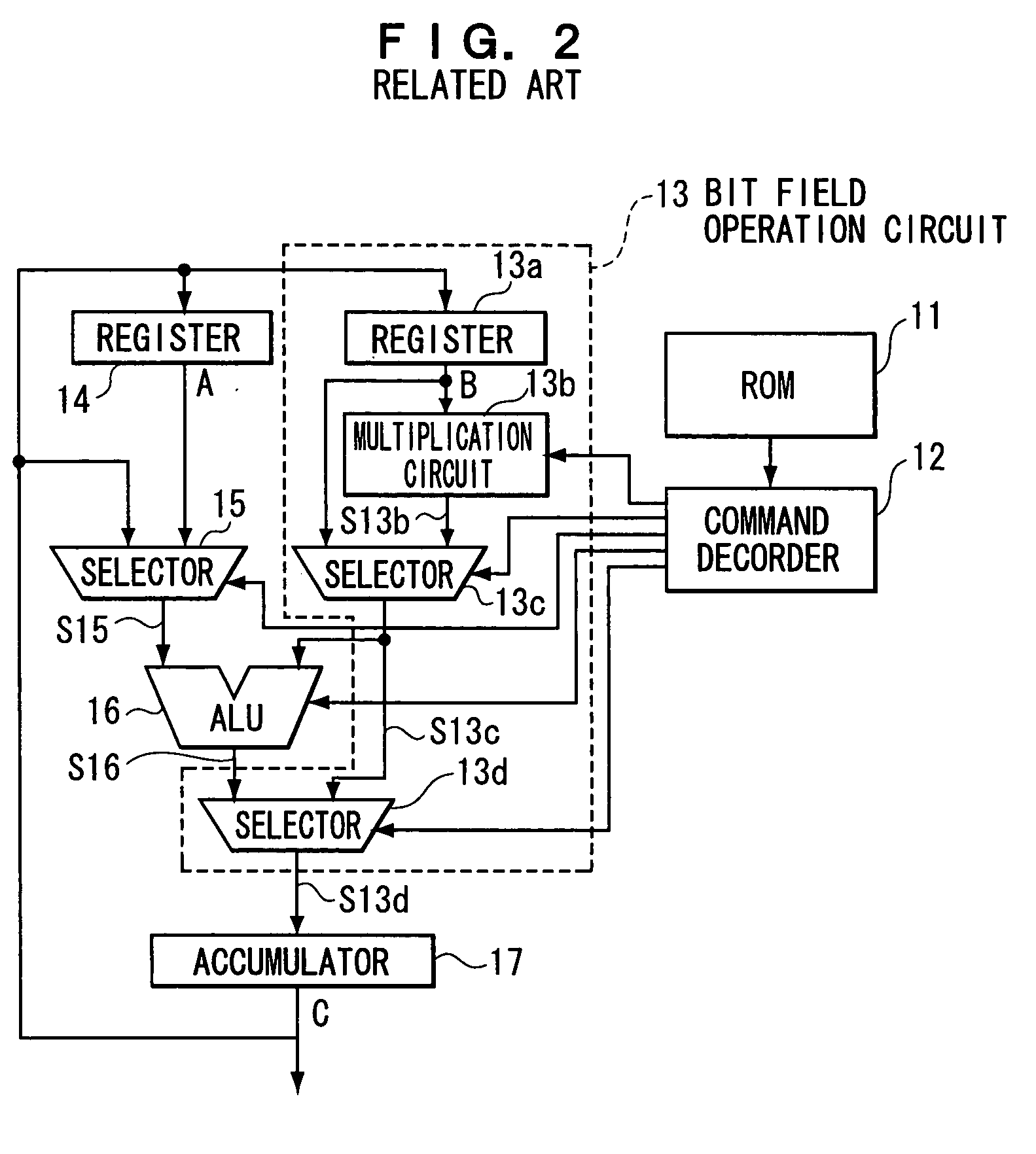
Accordingly, a processing amount within a fixed time is increased, a size of the ROM 11 is enlarged, and a manufacturing cost increase is caused.
Method used
Image
Click on the blue label to locate the original text in one second.
Reading with bidirectional positioning of images and text.
Examples
first embodiment
Effect of First Embodiment
[0055]In accordance with the present first embodiment, since the mask data generation circuit section 30 is provided, it is possible to generate the output data C in one cycle on the basis of the input data A and B, the reference data ref, the offset amount offset, the wide amount width, and the bit amount n. Accordingly, the cycle number of the bit field operation command is shortened to one sixth, a processing amount within a fixed time is reduced, a size of the ROM becomes small, and it is possible to reduce a manufacturing cost.
Second Embodiment
Structure of Second Embodiment
[0056]FIG. 10 is a schematic view of an outline of a bit field operation circuit showing an second embodiment in accordance with the invention. The common reference numerals are attached to the common elements with the elements in FIG. 1 showing the first embodiment.
[0057]The bit field operation circuit in accordance with the second embodiment is constituted by the same shifter 20 as...
second embodiment
Effect of Second Embodiment
[0070]In accordance with the present second embodiment, the mask data circuit is provided, and the NOR gate 35 is provided in place of the AND gate 34 in accordance with the first embodiment. Accordingly, approximately in the same manner as the first embodiment, the cycle number of the bit field operation command is shortened to one sixth, a processing amount within a fixed time is reduced, a size of the ROM becomes small, and it is possible to reduce a manufacturing cost.
modified embodiment
[0071]The invention is not limited to the first and second embodiments mentioned above, but can employ various applied aspects and can be variously modified. As the applied aspects and the modified embodiments, for example, there are the following structures such as (a) to (c).
[0072](a) The shifter 20 in FIGS. 1 and 10 is constituted by the shift computation circuit or the like, however, may be constituted by the other shift units such as a shift register or the like.
[0073](b) The AND gate 34 in FIG. 1 and the NOR gate 35 in FIG. 10 may be constituted by the other logic operation units such as an EXOR gate or the like. It is possible to expect the same effect as those of the first and second embodiments.
[0074](c) The selector 40 in accordance with FIGS. 1 and 10 is constituted by the multiplexer or the like, however, may be constituted by the other selection units.
[0075](d) The mask shift amount control circuit 31 in FIG. 5 is constituted by the adder 31a and the subtracter 31b, how...
PUM
Abstract
A bit field operation circuit has a first shift unit, a mask shift amount control circuit, a second shift unit, a logic operation unit, and a selection unit. The first shift unit outputs a first intermediate data based on a first control signal. The mask shift amount control circuit outputs a mask shift control signal in accordance with a mask shift amount. The second shift unit outputs a second intermediate data based on a mask shift control signal. The third shift unit outputs a third intermediate data based on the first control signal. The logic operation unit performs logical operation of the second intermediate data and the third intermediate data, and outputs a mask selection data. The selection unit selects either one of the first intermediate data or the second input data based on the mask selection data to output as output data.
Description
CROSS-REFERENCE TO RELATES APPLICATION[0001]This application claims priority under 35 USC 119 from Japanese Patent Application No. 2006-260613, the disclosure of which is incorporated by reference herein.BACKGROUND OF THE INVENTION[0002]1. Field of the Invention[0003]The present invention relates to a bit field operation circuit operating a bit field which is a bit row in which a length is smaller than n (n being an integer of 2 or more) (hereinafter, refer to as “bit”), in a processor such as a central processing unit (hereinafter, refer to as “CPU”), a microprocessor (hereinafter, refer to as “MPU”) having the CPU, a digital signal processor (hereinafter, refer to as “DSP”) having the CPU, a multiplication circuit or the like, and the like.[0004]2. Description of the Related Art[0005]Conventionally, as an example of a bit field operation circuit having a mask data generation circuit for generating a mask data used for executing a bit field operation, for example, there has been a ...
Claims
Application Information
Patent Timeline
Application Date:The date an application was filed.
Publication Date:The date a patent or application was officially published.
First Publication Date:The earliest publication date of a patent with the same application number.
Issue Date:Publication date of the patent grant document.
PCT Entry Date:The Entry date of PCT National Phase.
Estimated Expiry Date:The statutory expiry date of a patent right according to the Patent Law, and it is the longest term of protection that the patent right can achieve without the termination of the patent right due to other reasons(Term extension factor has been taken into account ).
Invalid Date:Actual expiry date is based on effective date or publication date of legal transaction data of invalid patent.

