JTAG boundary scan compliant testing architecture with full and partial disable

a testing architecture and boundary scan technology, applied in the field of semiconductor devices, can solve problems such as unauthorized users, difficulty in testing circuit boards and/or semiconductor devices,

Inactive Publication Date: 2008-04-03
AVAGO TECH WIRELESS IP SINGAPORE PTE
View PDF14 Cites 28 Cited by
  • Summary
  • Abstract
  • Description
  • Claims
  • Application Information

AI Technical Summary

Benefits of technology

[0007]A JTAG boundary scan compliant testing architecture with full and partial disable, substantially as show...

Problems solved by technology

Advances in semiconductor device packaging and circuit board manufacturing have made it very difficult to test the circuit board and/or the semiconductor devices by physically accessing or probing circuit board interconnects that connect semiconductor devices on a circuit board.
Disadvantageously, unauthoriz...

Method used


Image

  • JTAG boundary scan compliant testing architecture with full and partial disable
  • JTAG boundary scan compliant testing architecture with full and partial disable
  • JTAG boundary scan compliant testing architecture with full and partial disable

Examples


Embodiment Construction

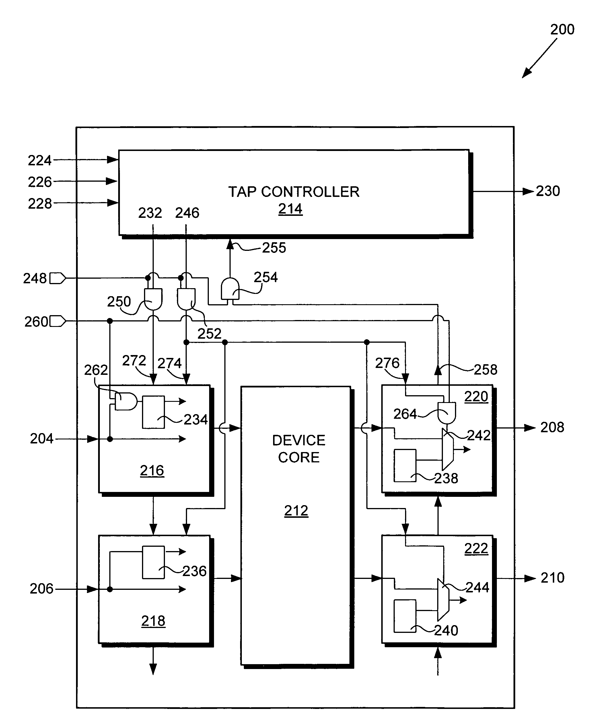
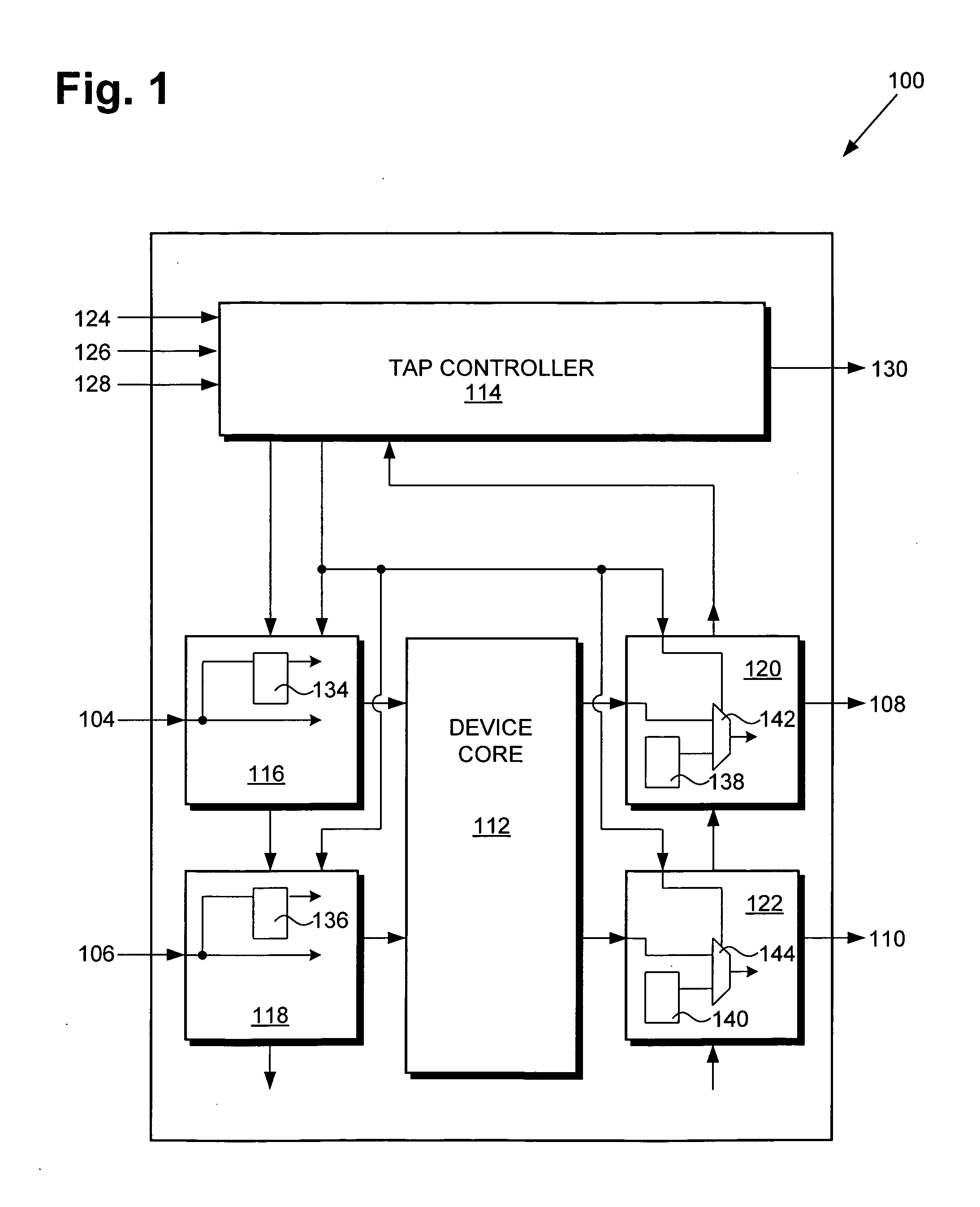
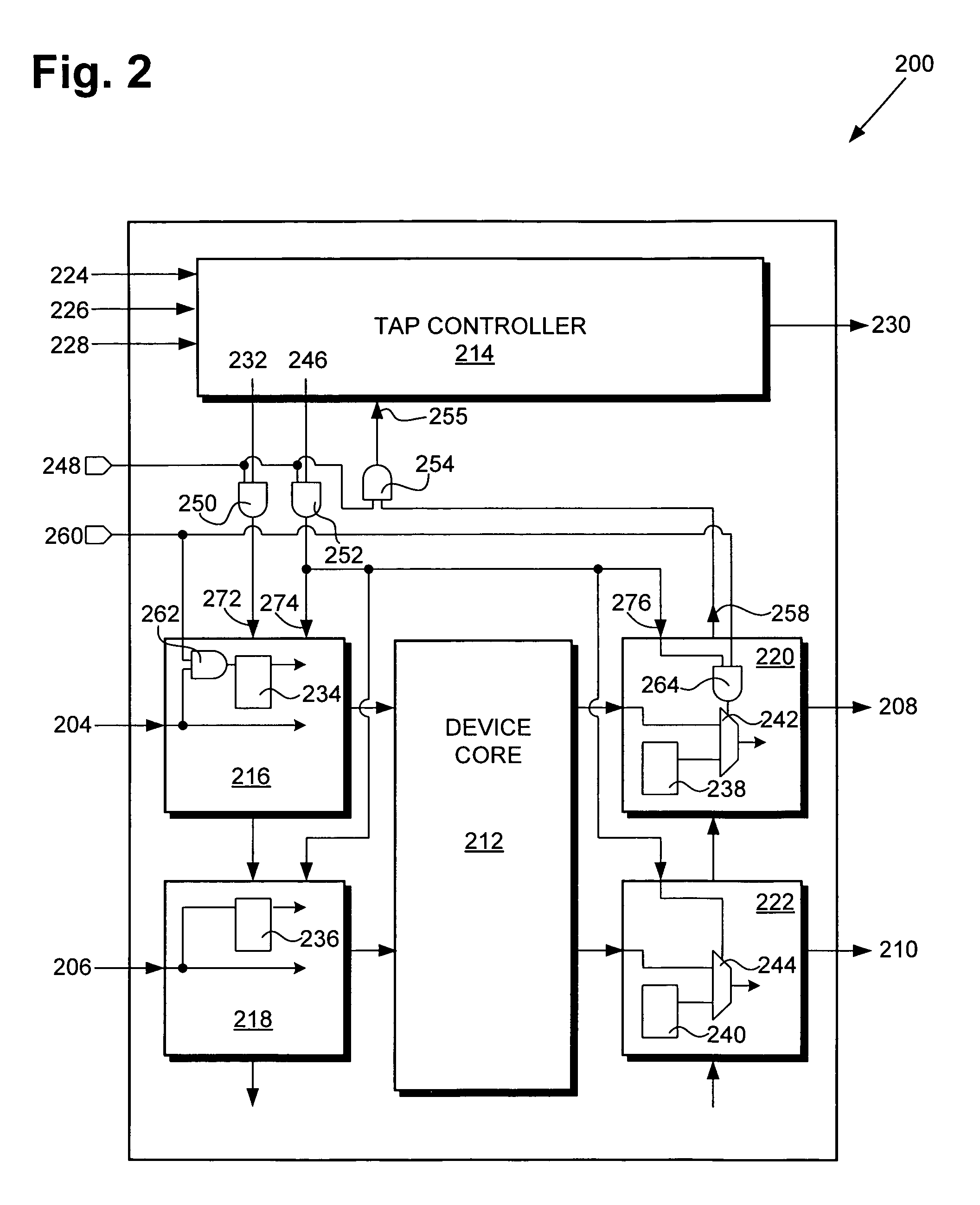
[0012]The present invention is directed to a JTAG boundary scan compliant testing architecture with full and partial disable capabilities. Although the invention is described with respect to specific embodiments, the principles of the invention, as defined by the claims appended herein, can obviously be applied beyond the specifically described embodiments of the invention described herein. Moreover, in the description of the present invention, certain details have been left out in order to not obscure the inventive aspects of the invention. The details left out are within the knowledge of a person of ordinary skill in the art.

[0013]The drawings in the present application and their accompanying detailed description are directed to merely exemplary embodiments of the invention. To maintain brevity, other embodiments of the invention which use the principles of the present invention are not specifically described in the present application and are not specifically illustrated by the p...


PUM


Abstract

A semiconductor device includes a JTAG boundary scan compliant testing architecture built into the semiconductor device, where the semiconductor device has a number of input points and output points. The JTAG boundary scan compliant testing architecture includes a TAP controller capable of receiving input test data, a test mode-select, and a test clock. In one embodiment, a full JTAG disable interface is utilized whereby the JTAG boundary scan compliant testing architecture allows an authorized user to prevent an unauthorized user from storing data into or reading data from input boundary scan registers and from reading data from output boundary scan registers. In another embodiment, a partial JTAG disable interface is utilized whereby an authorized user can prevent an unauthorized user from storing data into a pre-designated input boundary scan register, or from reading data from a pre-designated output boundary scan register.

Description

BACKGROUND OF THE INVENTION[0001]1. Field of the Invention[0002]The present invention is generally in the field of semiconductor devices. More specifically, the present invention is in the field of testing semiconductor devices.[0003]2. Background Art[0004]Advances in semiconductor device packaging and circuit board manufacturing have made it very difficult to test the circuit board and / or the semiconductor devices by physically accessing or probing circuit board interconnects that connect semiconductor devices on a circuit board. As a result, the Institute of Electrical and Electronic Engineers (“IEEE”) developed the IEEE 1149.1 standard, which includes a Joint Test Action Group (“JTAG”) boundary scan compliant testing architecture and provides means for, among other things, debugging and testing JTAG compliant devices on a circuit board without the need to physically probe the circuit board interconnects to access a particular device or a particular circuit board interconnect.[000...

Claims


Application Information

Patent Timeline
IPC IPC(8): G01R31/28
CPCG01R31/318536G01R31/318544G01R31/318563G01R31/318558G01R31/318561G01R31/318555
Inventor GUETTAF, AMAR
Owner AVAGO TECH WIRELESS IP SINGAPORE PTE
Why Eureka
Try Eureka