Solid-state imaging device

Inactive Publication Date: 2008-04-17
PANASONIC CORP
View PDF0 Cites 35 Cited by
  • Summary
  • Abstract
  • Description
  • Claims
  • Application Information

AI Technical Summary

Benefits of technology

[0021]In the second solid-state imaging device according to the present invention, the green pixel addition area is more preferably provided with a first green pixel addition area and a second pixel addition area, and the first green pixel addition area and the second green pixel addition area are more preferably arranged having a deviation of two pixels in the horizontal direction.
[0022]In the second solid-state imaging device according to the present invention, the first green pixel addition area and the second green pixel addition area are more preferably arranged to overlap the blue pixel addition area and the red pixel addition area.
[0023]In the second solid-state imaging device according to the present invention, the green pixel addition area is more preferably provided with a first green pixel addition area and a second green pixel addition area, and the first green pixel addition area and the second green pixel addition area are more preferably arranged in the same position in the horizontal direction.
[0024]In addition, the first

Problems solved by technology

However, there were cases where the solid-state imaging device of a nine-pixel addition system disclosed in the JP2004-312140 publication could not be used for imaging devices in which high-speed implementation and high pixelation are demanded to be compatible on a high level (e.g., single-lens digital still cameras), due to a large reduction in the number of added or mixed pix

Method used


Image

  • Solid-state imaging device
  • Solid-state imaging device
  • Solid-state imaging device

Examples


first embodiment

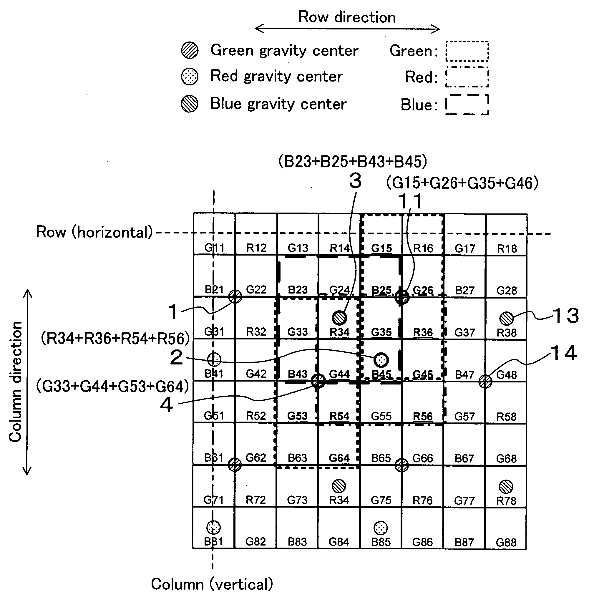
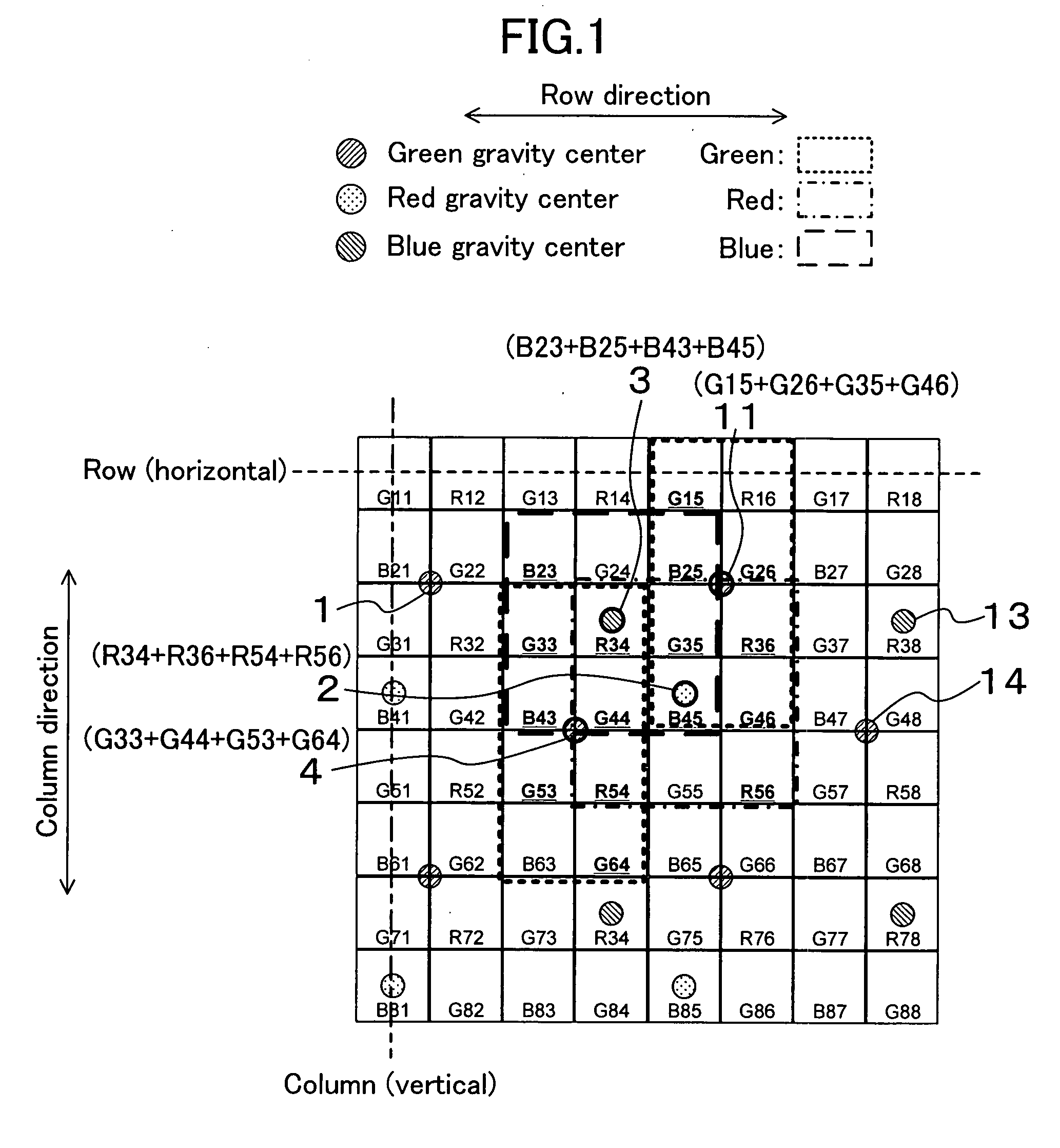
[0052]Explained below will be a solid-state imaging device and a driving method thereof according to a first embodiment of the present invention with reference to drawings.

[0053]FIG. 1 is an image diagram showing a pixel addition pattern of the solid-state imaging device and the driving method thereof according to the first embodiment of the present invention.

[0054]As shown in FIG. 1, a color filter array is a Bayer array, for example. A filter pixel held by an R filter on both horizontal sides is made to be Gr, and a filter pixel held by a B filter on both horizontal sides is made to be Gb for convenience of explaining an operation, but Gr and Gb are the same color in practice.

[0055]As shown in FIG. 1, green (hereinafter referred to as G) G15, G26, G35, and G46 are formed into a first G group, G33, G44, G53, and G64 are formed into a second G group, red (hereinafter referred to as R) R34, R54, R36, and R56 are formed into an R group, blue (hereinafter referred to as B) B23, B25, B4...

modified example 1 of first embodiment

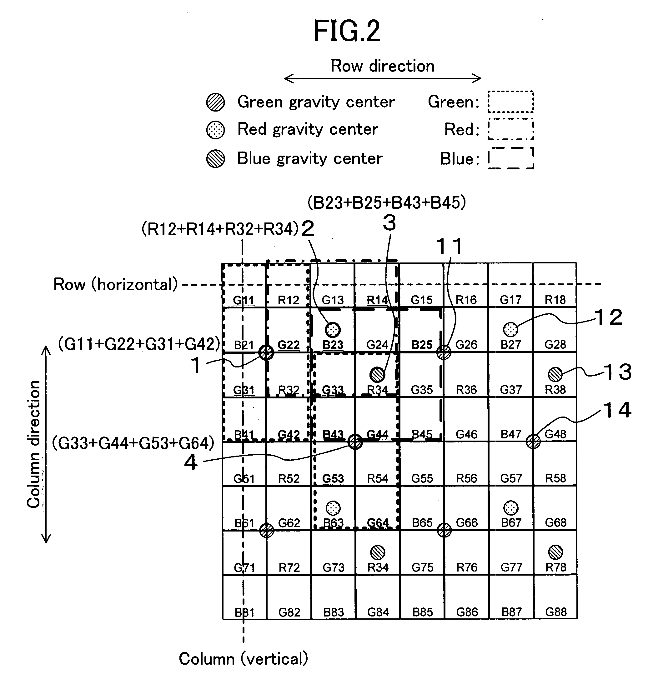
[0101]A solid-state imaging device and a driving method thereof according to a modified example 1 of the first embodiment of the present invention will be explained below by referring to a diagram. Any one of the first to fourth configurations of the solid-state imaging device according to the first embodiment as shown in FIG. 5, FIG. 7, FIG. 10, and FIG. 15 is used for a device configuration of the solid-state imaging device according to this modified example 1.

[0102]FIG. 2 is an image diagram showing a pixel addition pattern of the solid-state imaging device and the driving method thereof according to the modified example 1 of the first embodiment of the present invention.

[0103]As shown in FIG. 2, a color filter array is a Bayer array, for example, in which a filter pixel held by an R filter on both horizontal sides is made to be Gr, and a filter pixel held by a B filter on both horizontal sides is made to be Gb for convenience of explaining an operation, but Gr and Gb are the sam...

modified example 2 of first embodiment

[0105]A solid-state imaging device and a driving method thereof according to a modified example 2 of the first embodiment of the present invention will be explained below by referring to a diagram. Any one of the first to fourth configurations of the solid-state imaging device according to the first embodiment of the present invention as shown in FIG. 5, FIG. 7, FIG. 10, and FIG. 15 is used for a device configuration of the solid-state imaging device according to this modified example 2 of the first embodiment of the present invention.

[0106]FIG. 3 is an image diagram showing a pixel addition pattern of the solid-state imaging device and the driving method thereof according to the modified example 2 of the first embodiment of the present invention.

[0107]As shown in FIG. 3, a color filter array is a Bayer array, for example, in which a filter pixel held by an R filter on both horizontal sides is made to be Gr, and a filter pixel held by a B filter on both horizontal sides is made to b...


PUM


Abstract

An amplification-type solid-state imaging device adds a plurality of signals from pixels of the same color, R, G, or B, in order to output the signals. A gravity center in each group of added pixels is arranged without being partial in a pixel region.

Description

BACKGROUND OF THE INVENTION[0001]1. Technical Field[0002]The present invention relates to a solid-state imaging device with a pixel addition mode.[0003]2. Related Art[0004]Further improvement in image quality and functions is demanded in imaging devices such as digital still cameras, and solid-state imaging devices mounted on the imaging devices employ a technique to implement a high speed by a pixel addition or pixel mixture method. Explanation will be made for a solid-state imaging device according to a conventional technique disclosed in Japanese Patent Application Publication No. 2004-312140, the entire contents of which being herein incorporated in reference, with reference to drawings.[0005]FIG. 25 is a configuration diagram of the solid-state imaging device disclosed in Japanese Patent Application Publication No. 2004-312140.[0006]Reference numeral 1011 is a photoelectric conversion element and a color filter attached to a front surface thereof. It is assumed here that a colo...

Claims


Application Information

Patent Timeline
IPC IPC(8): H04N3/14H01L27/146H04N5/335H04N5/347H04N5/357H04N5/369H04N5/374H04N5/3745H04N9/07
CPCH04N3/1506H04N5/3458H04N9/045H04N5/37457H04N5/347H04N25/46H04N25/766H04N25/778H04N25/70H04N25/447H04N25/76H04N25/75H04N25/134
Inventor MATSUNAGA, YOSHIYUKI
Owner PANASONIC CORP
Why Eureka
Try Eureka