Solid-state imaging device and method for manufacturing the same

A solid-state imaging device, a horizontal technology, applied in the direction of electric solid-state devices, radiation control devices, semiconductor devices, etc., can solve the problems of limited drive pulse delay, inability to increase, and dielectric breakdown strength (reduced insulation withstand voltage, etc.)

Inactive Publication Date: 2007-04-25
PANASONIC CORP
View PDF1 Cites 0 Cited by
  • Summary
  • Abstract
  • Description
  • Claims
  • Application Information

AI Technical Summary

Problems solved by technology

However, an increase in film thickness is accompanied by problems in processing such as etching, and a problem of deterioration in light collection efficiency due to an increase in the height (thickness dimension) of the element.
[0014] In addition, the increase in phosphorus doping is limited and cannot be increased above the limit of solid solubility
In addition, the insulation of the horizontal transfer electrodes 110 and 111 is performed by the oxide film obtained by thermally oxidizing the horizontal transfer electrode 110. However, if the phosphorus doping amount increases, the thickness of the oxide film becomes thicker, and the transfer efficiency deteriorates due to the increase in the distance between the transfer electrodes.
In addition, if the amount of oxidation is the same as in the prior art, the phosphorus concentration in the oxide film will increase, which will lead to a decrease in dielectric breakdown strength (dielectric withstand voltage).
Therefore, the polysilicon forming the horizontal transfer electrodes 110 and 111 also has a limit to the suppression of the driving pulse delay due to the increase of impurities.

Method used


Image

  • Solid-state imaging device and method for manufacturing the same
  • Solid-state imaging device and method for manufacturing the same
  • Solid-state imaging device and method for manufacturing the same

Examples


Embodiment approach 1

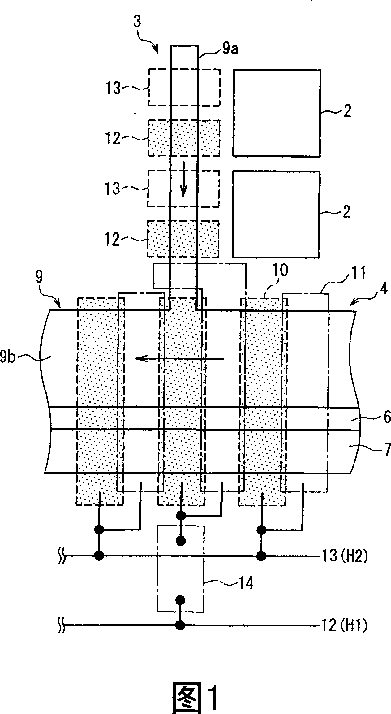
[0044] FIG. 1 is a plan view schematically showing the configuration of a solid-state imaging device according to Embodiment 1 of the present invention.

[0045] As shown in FIG. 1 , the solid-state imaging device according to Embodiment 1 is a CCD-type solid-state imaging device formed on a semiconductor substrate. Similar to the conventional examples shown in FIGS. 6 to 8 in the description of the background art, a plurality of light receiving sections 2 arranged in a two-dimensional matrix and a plurality of light receiving sections 2 along the semiconductor substrate (101 in FIG. 6 ) are provided on a semiconductor substrate (101 in FIG. 6 ). The vertical transfer unit (vertical CCD) 3 is arranged for each column in the vertical direction. In addition, a horizontal transfer unit (horizontal CCD) 4 is provided so as to be adjacent to the final row of the vertical transfer unit 3 .

[0046] The light receiving unit 2 is constituted by a photodiode, and stores charges accord...

Embodiment approach 2

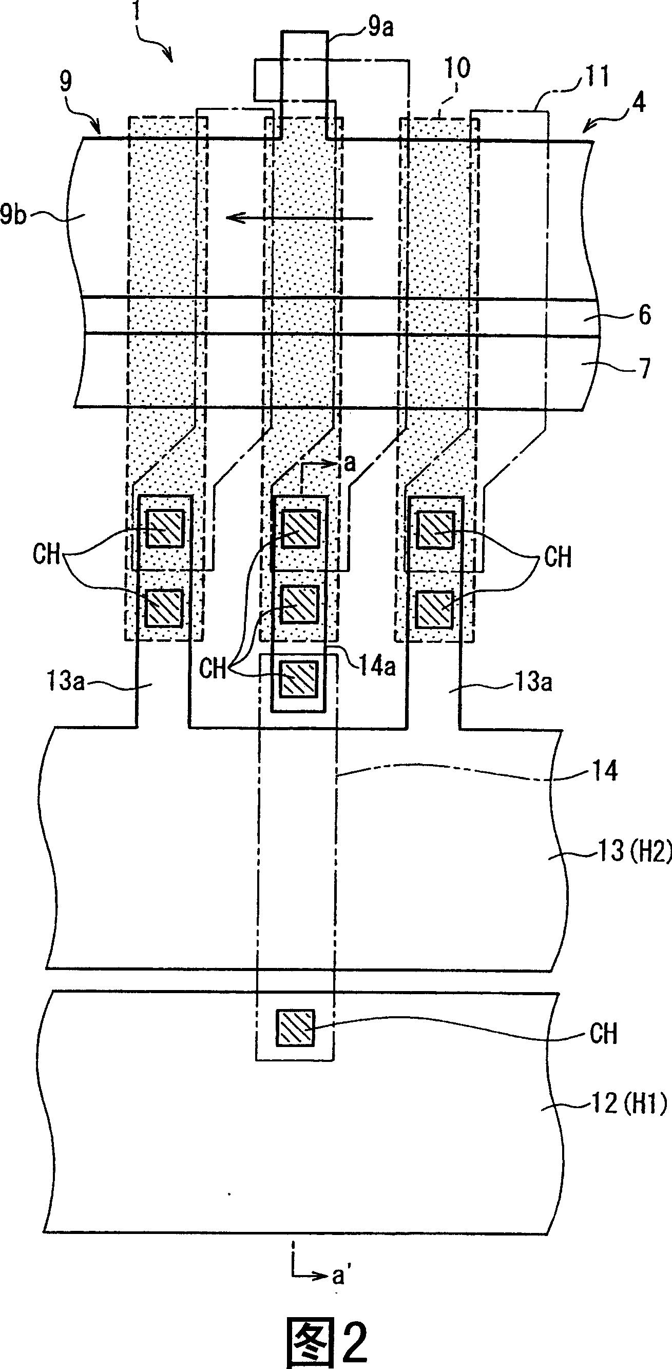
[0057] 5 is a plan view schematically showing the configuration of a solid-state imaging device according to a second embodiment of the present invention.

[0058] As shown in FIG. 5 , in the solid-state imaging device of the present embodiment, a discharge region connection portion 15 for applying a voltage to the discharge region 7 is provided for each horizontal CCD 4 , and a connection between the discharge region connection portion 15 and the power supply line is provided. The discharge contact area 16 of the connecting portion.

[0059] By disposing in this way, with respect to the discharge region 7, it is possible to suppress an increase in impurities due to deterioration of the withstand voltage due to a decrease in the resistance value that determines the discharge capability, or an increase in the discharge area due to an increase in the load capacitance. . As a result, the area of ​​the thin film region of the insulating film covering the horizontal transfer elect...


PUM


Abstract

The solid-state imaging device of the present invention includes: a plurality of photodetectors that are arranged in a two-dimensional matrix; a plurality of vertical transfer portions that transfer, in a vertical direction, signal electric charges which are read out from the respective photodetectors; a horizontal transfer portion that receives the signal electric charges transferred by the vertical transfer portions, and transfers the signal electric charges in a horizontal direction; a barrier region that is adjacent to the horizontal transfer portion, and allows an excess electric charge in the horizontal transfer portion to pass through; and a drain region that is adjacent to the barrier region and drains the excess electric charge which has passed through the barrier region; and bus lines that are disposed in parallel with the drain region, and apply control voltages to electrodes of the horizontal transfer portion. The bus lines and the electrodes of the horizontal transfer portion are connected via a connection pattern that is disposed between the bus lines and the drain region. A power loss in the horizontal transfer portion is suppressed, and both of an increase in the number of pixels and a decrease in power consumption are achieved.

Description

technical field [0001] The present invention relates to a solid-state imaging device and a manufacturing method thereof, and more particularly to a CCD (CHARGE COUPLING DEVICE: Charge Coupled Device) type solid-state imaging device and a manufacturing method thereof. Background technique [0002] In recent years, solid-state imaging devices are mounted on digital cameras and digital video cameras, and demand is increasing. In addition, among portable terminal devices typified by mobile phones, there are more and more types having a camera function. Demand for solid-state imaging devices has also increased as imaging devices for such portable terminal devices. Furthermore, in order to obtain high-quality images, the number of pixels of solid-state imaging devices tends to increase. In addition, with the reduction in power consumption of digital cameras, digital video cameras, portable terminal devices, and the like, there is an increasing demand for low power consumption of...

Claims


Application Information

Patent Timeline
Patent Type & Authority Applications(China)
IPC IPC(8): H01L27/148H01L23/522
CPCH01L27/14812H01L29/768
Inventor 栗山俊宽
Owner PANASONIC CORP
Why Eureka
Try Eureka