Array quad flat no-lead package and method of forming same

a flat no-lead, array technology, applied in the direction of electrical apparatus, semiconductor devices, semiconductor/solid-state device details, etc., can solve the problems of increasing the likelihood of cross-talk and signal interference, reducing the number of i/o connections on such packages, and complicating the manufacturing process

Active Publication Date: 2008-05-01
NORTH STAR INNOVATIONS
View PDF5 Cites 8 Cited by
  • Summary
  • Abstract
  • Description
  • Claims
  • Application Information

AI Technical Summary

Problems solved by technology

A drawback, however, is that the number of I/O connections on such packages is limited.
Unfortunately, the reduction ...

Method used


Image

  • Array quad flat no-lead package and method of forming same
  • Array quad flat no-lead package and method of forming same
  • Array quad flat no-lead package and method of forming same

Examples


Embodiment Construction

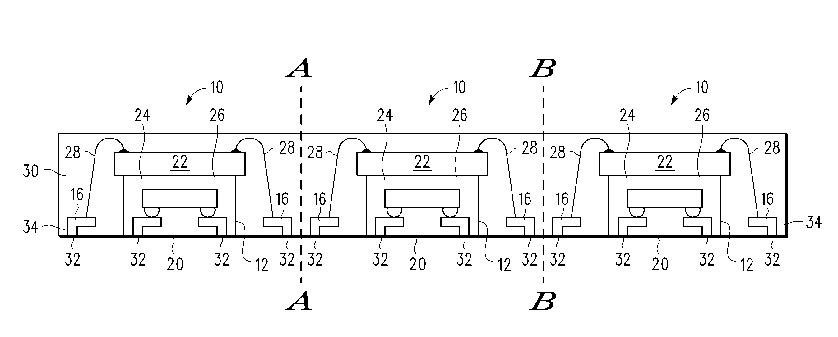
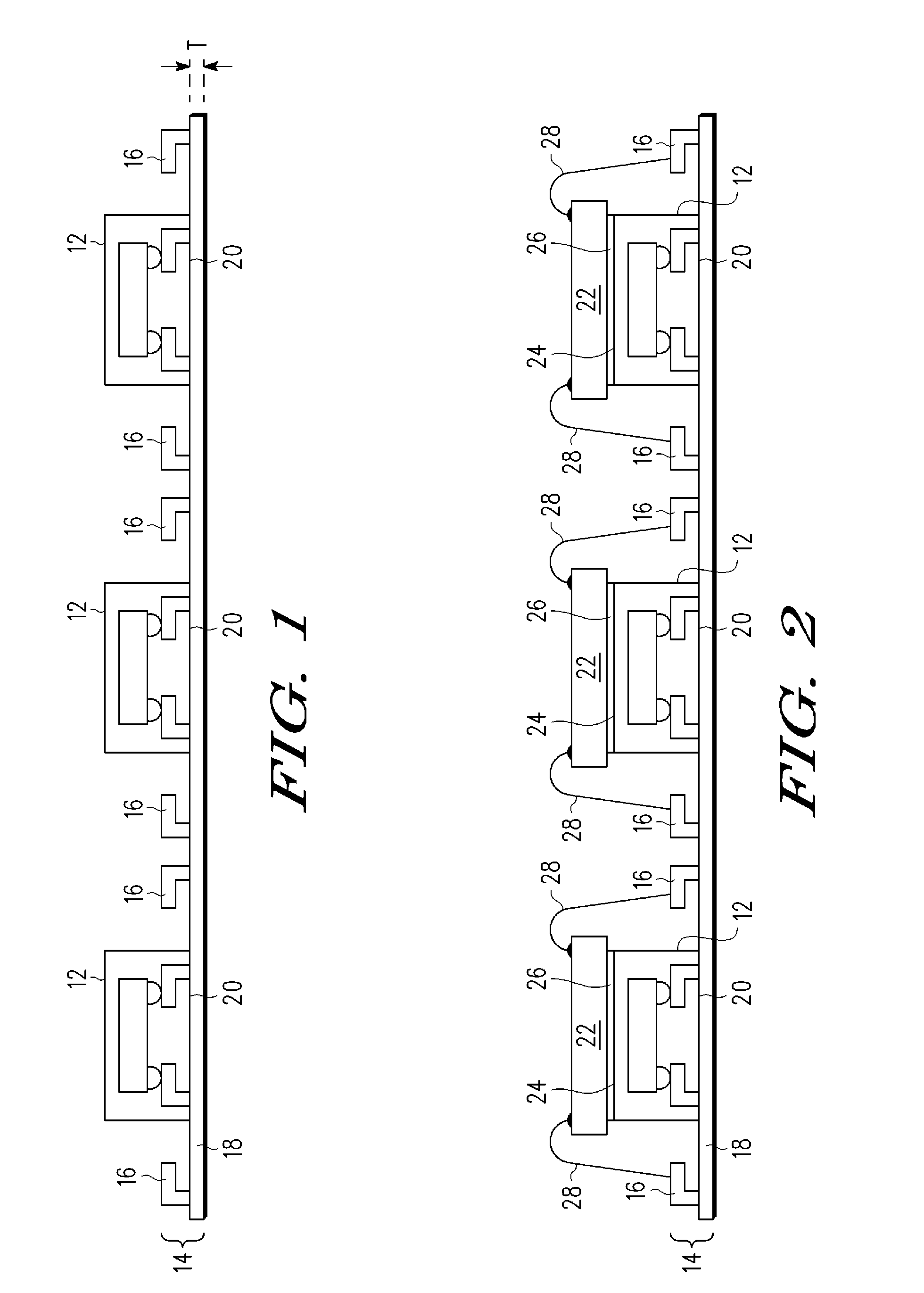
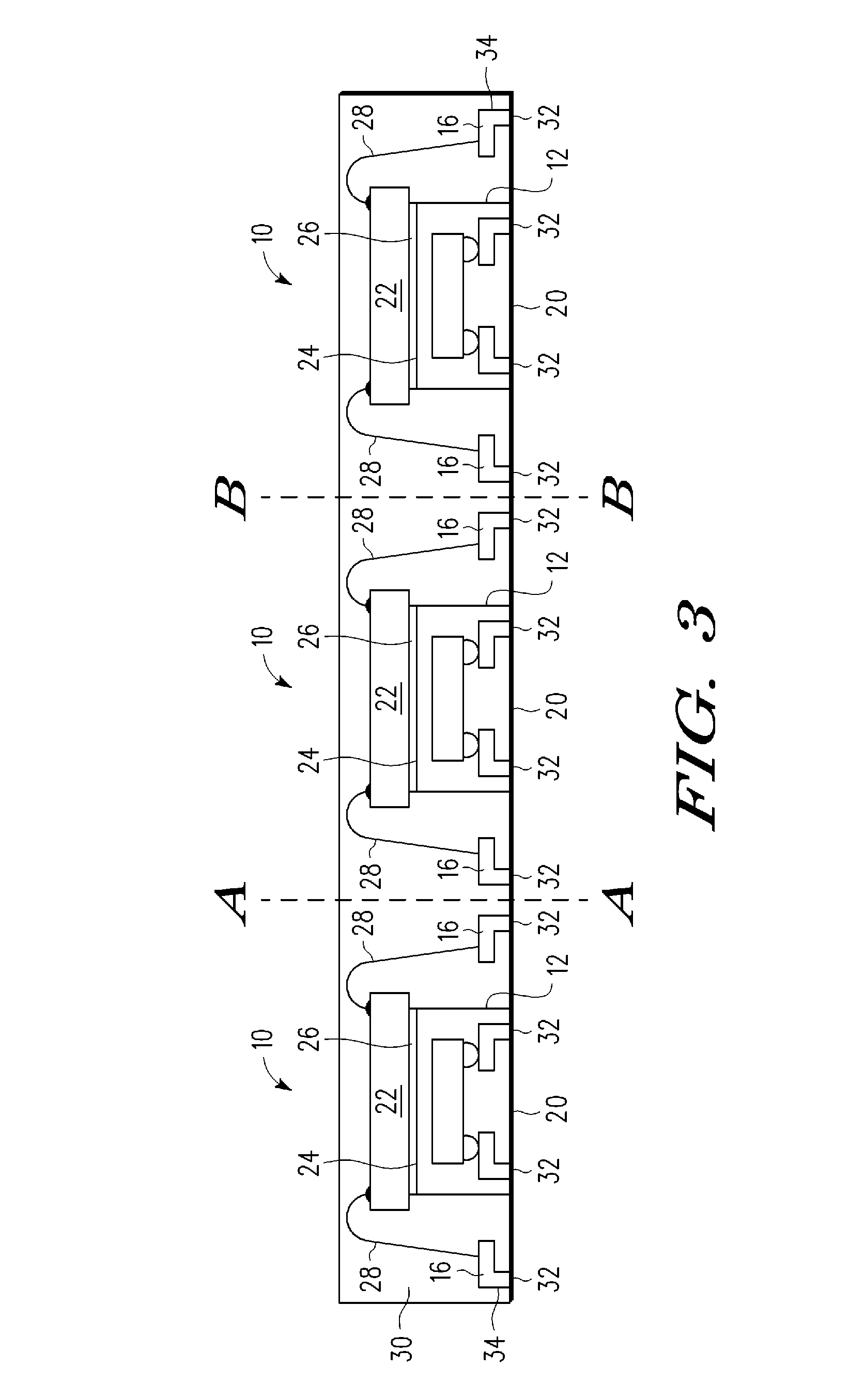
[0009]The detailed description set forth below in connection with the appended drawings is intended as a description of the presently preferred embodiments of the invention, and is not intended to represent the only form in which the present invention may be practiced. It is to be understood that the same or equivalent functions may be accomplished by different embodiments that are intended to be encompassed within the spirit and scope of the invention. In the drawings, like numerals are used to indicate like elements throughout.

[0010]The present invention provides a semiconductor package including a first semiconductor package, and a lead frame having a plurality of leads. A first IC die is attached on a first side to the first semiconductor package and electrically connected to the leads of the lead frame. The first IC die, a portion of the first semiconductor package and a portion of the leads are encapsulated by a mold compound such that a plurality of input and output (IO) term...


PUM


Abstract

An array QFN package (10) includes a first semiconductor package (12) and a lead frame (14) having a plurality of leads (16). A first IC die (22) is attached on a first side to the first semiconductor package (12) and is electrically connected to the leads (16) of the lead frame (14). A mold compound (30) encapsulates the first IC die (22), a portion of the first semiconductor package (12) and a portion of the leads (16) such that a plurality of I/O terminals (32) on the semiconductor package (10) is exposed.

Description

BACKGROUND OF THE INVENTION[0001]The present invention relates to the packaging of integrated circuits (ICs) and more particularly to an array quad flat no-lead (QFN) package and a method of forming the array QFN package.[0002]A conventional QFN package typically comprises an IC die attached and electrically connected to a lead frame. The IC die, the electrical connections and a portion of the lead frame are encapsulated by a mold compound, leaving a portion of the leads exposed. The exposed leads serve as input and output (IO) connections to the encapsulated IC die and are typically located along a periphery of the QFN package. Because QFN packages provide a number of advantages over other lead frame package configurations including, for example, shorter electrical paths and faster signal communication rates, QFN packages are widely used as low pin count solutions for power elements. A drawback, however, is that the number of I / O connections on such packages is limited. Increasing ...

Claims


Application Information

Patent Timeline
IPC IPC(8): H01L31/00
CPCH01L21/561H01L2224/32145H01L23/3107H01L24/97H01L2224/48091H01L2224/73265H01L2224/97H01L2924/01047H01L2924/01079H01L2924/01082H01L2924/01322H01L2924/14H01L2924/1433H01L21/568H01L2224/16245H01L2224/32225H01L24/48H01L2224/48247H01L2924/01033H01L2924/01006H01L2924/01005H01L2924/00014H01L2224/85H01L2224/81H01L2224/83H01L2924/00H01L2924/181H01L2224/32245H01L2924/00011H01L2224/0401H01L2924/00012H01L2224/45099H01L2224/45015H01L2924/207
Inventor LO, WAI YEWYIP, HENG KEONG
Owner NORTH STAR INNOVATIONS
Why Eureka
Try Eureka