Electron emission display

Inactive Publication Date: 2008-05-08
SAMSUNG SDI CO LTD
View PDF1 Cites 4 Cited by
  • Summary
  • Abstract
  • Description
  • Claims
  • Application Information

AI Technical Summary

Benefits of technology

[0023]Some embodiments provide a method for improving an accuracy of color reproduction in an electron emission display, the method comprising: disposing a spacer between a first substrate and a second su

Problems solved by technology

These changes in the electron beam path around the spacers reduce the accura

Method used


Image

  • Electron emission display
  • Electron emission display
  • Electron emission display

Examples


Embodiment Construction

[0028]With reference to the accompanying drawings, certain embodiments are described in sufficient detail for those skilled in the art to implement. As those skilled in the art would realize, the described embodiments may be modified in various different ways, all without departing from the spirit or scope of the disclosure. Wherever possible, like reference numbers in the drawings to refer to similar or like parts.

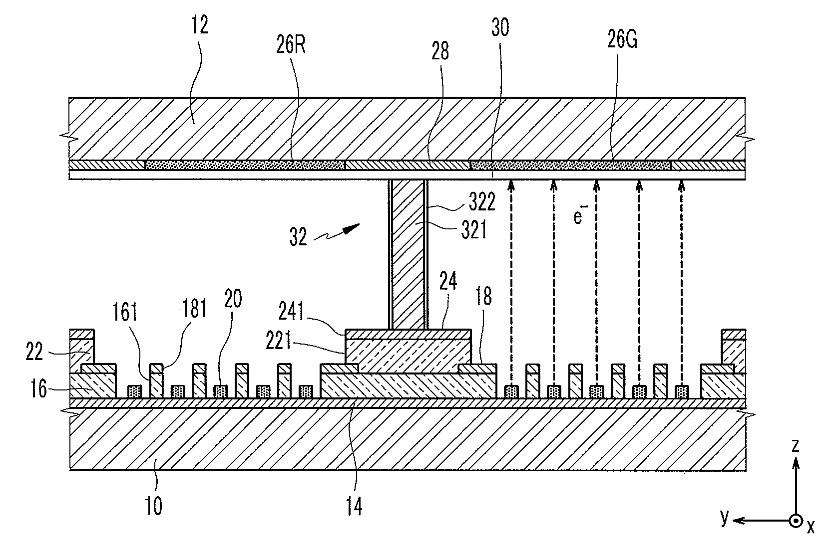
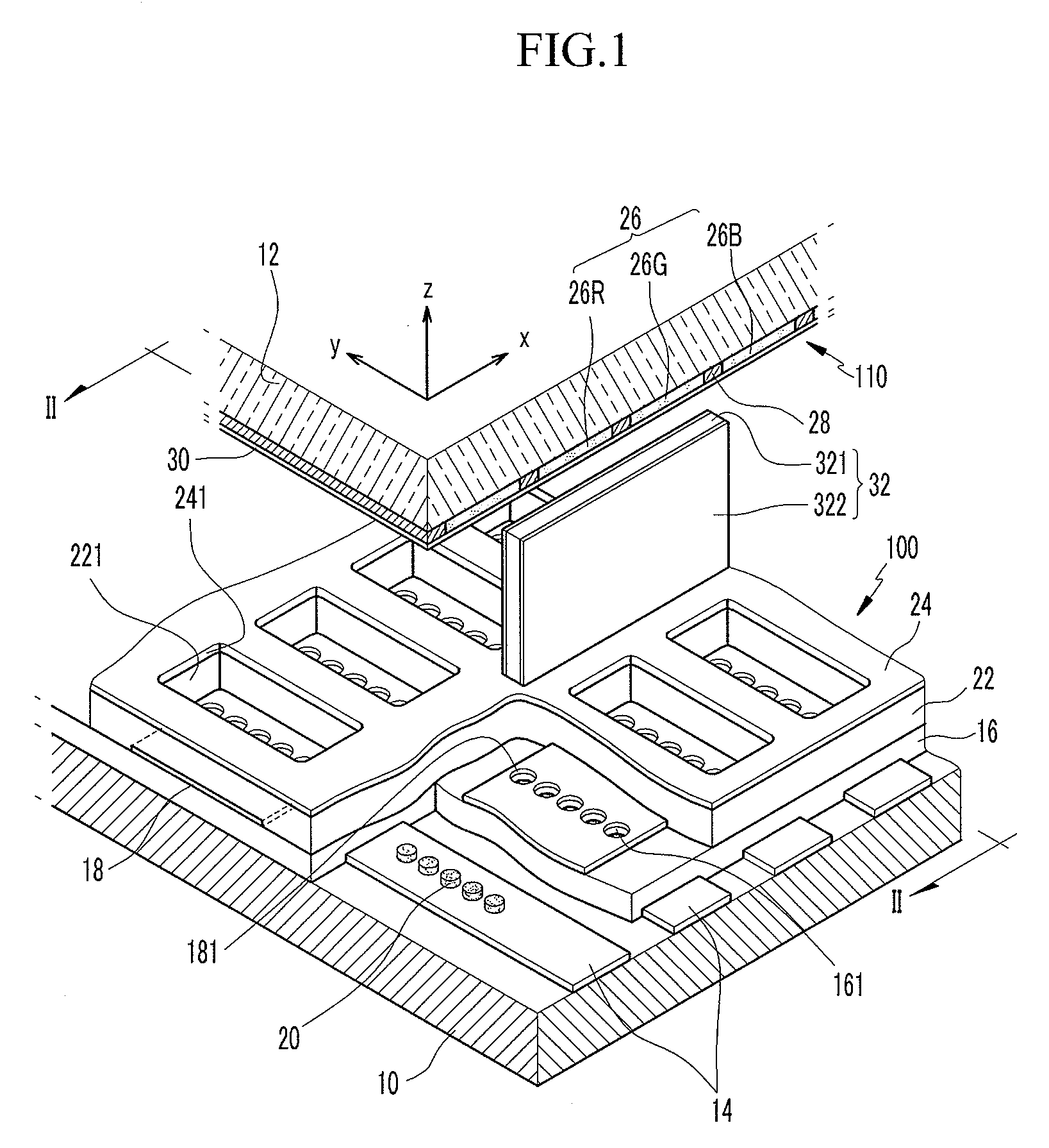
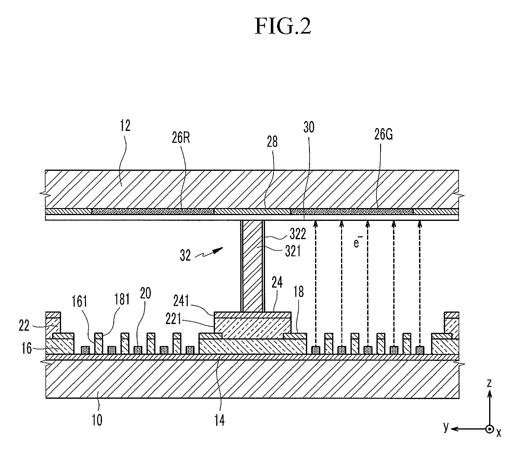
[0029]FIG. 1 is a partially exploded perspective view of an embodiment of an electron emission display. FIG. 2 is a cross-sectional view taken along line II-II of FIG. 1. Referring to FIGS. 1 and 2, the illustrated electron emission display includes first 10 and 12 second substrates opposing each other, generally in parallel at a predetermined distance. The first 10 and second 12 substrates are sealed together at their peripheries using a sealing member (not shown) to provide a vacuum vessel. The interior of the vacuum vessel is evacuated to about 10−6 Torr.

[0030]An elect...


PUM


Abstract

An electron emission display includes first and second substrates opposing each other, an electron emission unit that is provided on an inner surface of the first substrate, a light emission unit that is provided on an inner surface of the second substrate, and a spacer that is located between the first and second substrate. The spacer includes a main body containing a material whose temperature-coefficient-of-resistance is less than or equal to 3%/° C.

Description

CROSS-REFERENCE TO RELATED APPLICATION[0001]This application claims the benefit of Korean Patent Application No. 10-2006-0107746, filed on Nov. 2, 2006 in the Korean Intellectual Property Office, the disclosure of which is incorporated herein by reference.BACKGROUND[0002]1. Technical Field[0003]This disclosure relates generally to an electron emission display, and more particularly, to and an electron emission display comprising spacers that are installed in a vacuum vessel that counteract compression of the vacuum vessel.[0004]2. Description of Related Art[0005]Generally, electron emission elements are classified into those using hot cathodes as electron emission sources and those using cold cathodes as electron emission sources. Known cold cathode electron emission elements include, Field Emitter Array (FEA) electron emission elements, Surface-Conduction-Emission (SCE) electron emission elements, Metal-Insulator-Metal (MIM) electron emission elements, and Metal-Insulator-Semicondu...

Claims


Application Information

Patent Timeline
IPC IPC(8): H01J1/62H01J29/02
CPCH01J29/86H01J29/864H01J2329/8645H01J2329/864H01J31/127H01J1/30H01J31/12
Inventor JEONG, SEUNG-HEE
Owner SAMSUNG SDI CO LTD
Why Eureka
Try Eureka