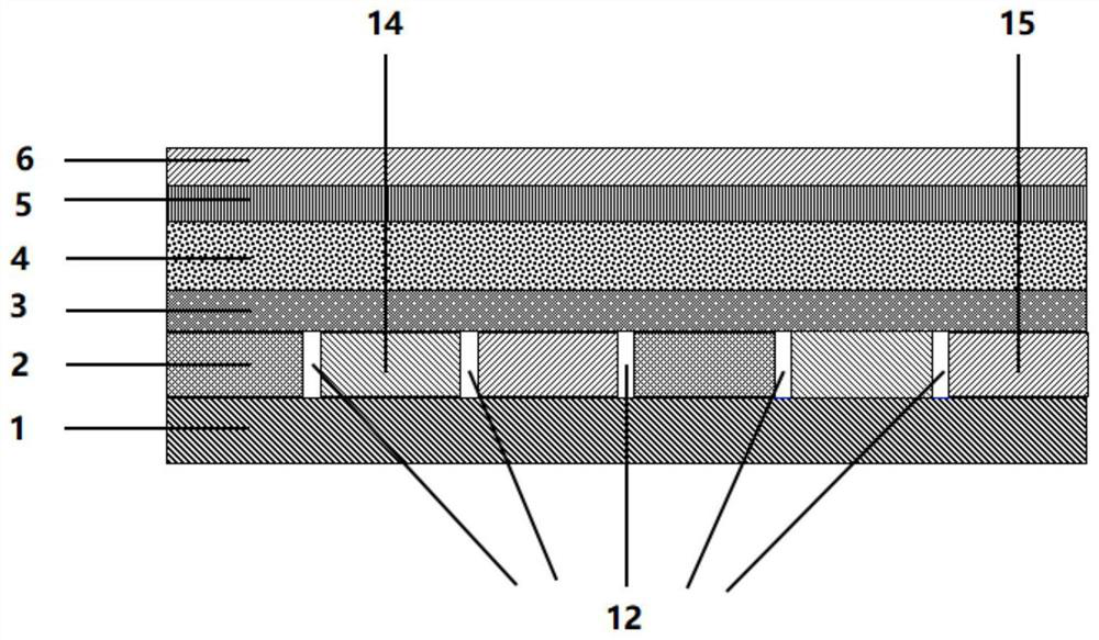
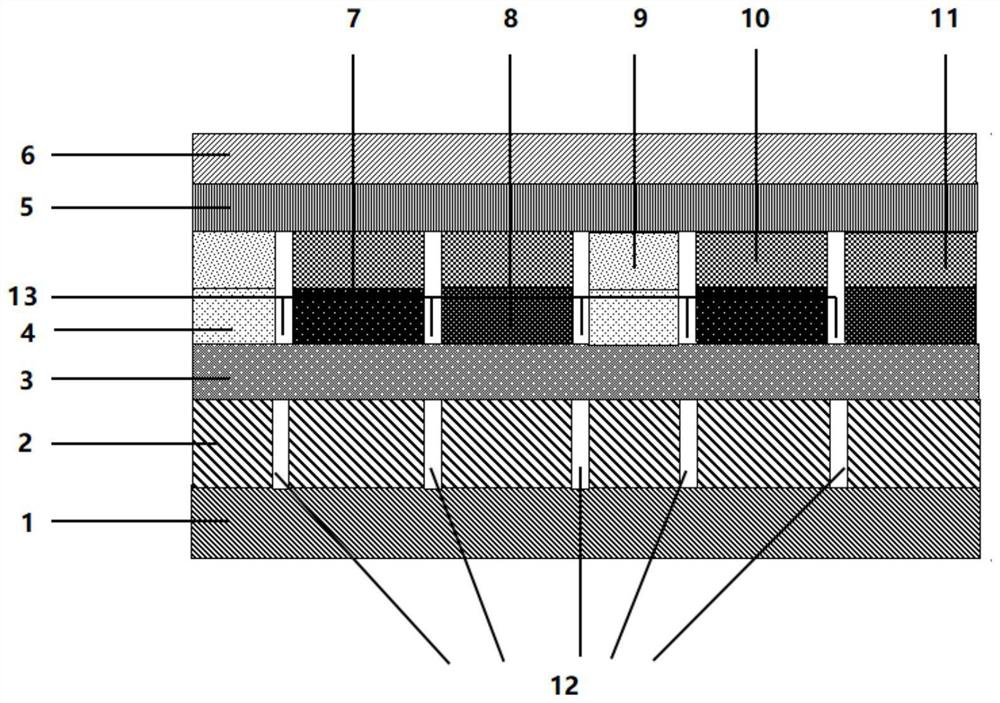
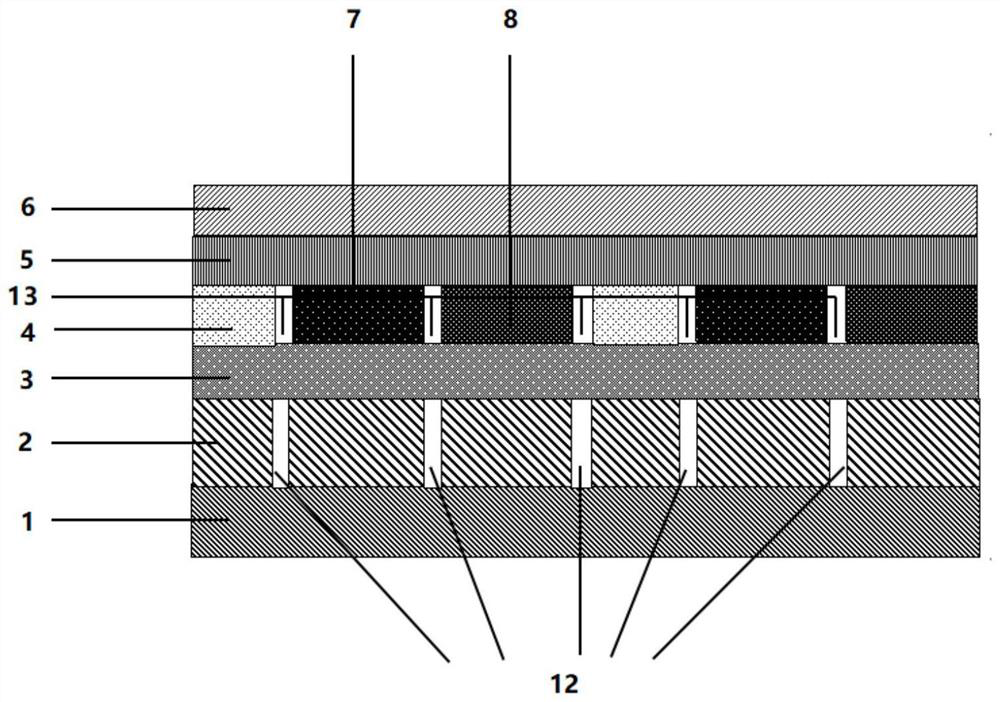
A full-color organic electroluminescence device
A luminescence, red light-emitting technology, applied in the direction of circuits, electrical components, electric solid-state devices, etc., can solve the problem of color shift of RGB three-primary color devices, achieve high color accuracy, improve display effect, and improve cost performance
- Summary
- Abstract
- Description
- Claims
- Application Information
AI Technical Summary
Problems solved by technology
Method used
Image
Examples
manufacture Embodiment 1
[0099] Manufacturing steps process:
[0100] (1) On the control circuit 1, a reflective electrode layer 2a with a thickness of ITO(7nm) / Ag(100nm) / ITO(7nm) was fabricated by magnetron sputtering, and its film resistance was 9Ω / □. Subsequently, the reflective electrode layer 2a is patterned, and the first electrode isolation column and the second electrode isolation column are fabricated on the processed reflective electrode, wherein the first electrode isolation column has a trapezoidal structure, and the second trapezoidal isolation column is an inverted structure. Ladder structure. All the reflective electrode patterns and the isolation columns of the first electrode are processed by the same photolithography process used in traditional liquid crystal panels. The photoresist material used for the first electrode isolation column and the second electrode isolation column is ZPN1168 photoresist material produced by Zeon Co., Ltd. of Japan.
[0101] (2) After completing the fa...
manufacture Embodiment 2
[0130] Complete the entire full-color OLED light-emitting device according to the steps of Manufacturing Example 1, the difference is that in the preparation process of the blue OLED device, the process of step e) and step d) is repeated after step f) to form a three-layer blue OLED light-emitting device;
manufacture Embodiment 3
[0132] Complete the whole full-color OLED light-emitting device according to the steps of Manufacturing Example 1, the difference is that LiF in steps (3) and (6) is replaced by BaF 2 ;
PUM
| Property | Measurement | Unit |
|---|---|---|
| luminescence spectroscopy | aaaaa | aaaaa |
| thickness | aaaaa | aaaaa |
| thickness | aaaaa | aaaaa |
Abstract
Description
Claims
Application Information


