Fanout line structure and flat display device including fanout line structure

a technology of fanout line and flat display device, which is applied in the direction of logic circuit, pulse technique, instruments, etc., can solve the problems of reducing image quality, difficult to realize the process in practice, and difference in resistance level of fanout line, so as to reduce the difference in resistance level

Inactive Publication Date: 2008-06-12
SAMSUNG DISPLAY CO LTD
View PDF4 Cites 74 Cited by
  • Summary
  • Abstract
  • Description
  • Claims
  • Application Information

AI Technical Summary

Benefits of technology

[0008]According to one aspect, the invention is a fanout line structure that connects a signal line to a bonding pad and includes a plurality of fanout lines that are disposed apart from each other. The plurality of fanout lines are formed to have different lengths, and a hole pattern is formed in at least one of the plurality of fanout lines to reduce the difference in resistance levels between the fanout lines.
[0015]In another aspect, the present invention is a flat display panel that includes a signal line formed on a substrate, a bonding pad that receives a driving signal, and a fanout line part that electrically connects the signal line to the bonding pad. The fanout line part includes a plurality of fanout lines that are apart from each other, the plurality of fanout lines are formed to have different lengths, and a hole pattern is formed in at least one of the plurality of fanout lines to reduce the difference in resistance levels between the fanout lines.
[0016]According to still another aspect, the present invention is a flat display device including a signal line formed on a substrate, a bonding pad that receives a driving signal, and a fanout line part that electrically connects the signal line to the bonding pad, and a driving circuit unit that includes a driving IC driving the flat display panel. The fanout line part includes a plurality of fanout lines that are positioned apart from each other, the plurality of fanout lines are formed to have different lengths, and a hole pattern is formed in at least a portion of the plurality of fanout lines to reduce the difference in resistance levels between the fanout lines.

Problems solved by technology

This difference in the length of the fanout lines causes a difference in the resistance levels of the fanout lines.
Due to the difference in resistance, the signal applied to the signal line of the pixel region is sometimes distorted, reducing the image quality.
However, it is difficult to realize the process in practice because the gradual change in the widths of fanout lines is not a desirable design for masks.
Accordingly, it is difficult to compensate for the different resistance levels in the fanout lines using this tapered-line theory.

Method used


Image

  • Fanout line structure and flat display device including fanout line structure
  • Fanout line structure and flat display device including fanout line structure
  • Fanout line structure and flat display device including fanout line structure

Examples


Embodiment Construction

[0024]Exemplary embodiments of the invention are described more fully hereinafter with reference to the accompanying drawings. This invention may, however, be embodied in many different forms and should not be construed as limited to the embodiments set forth herein.

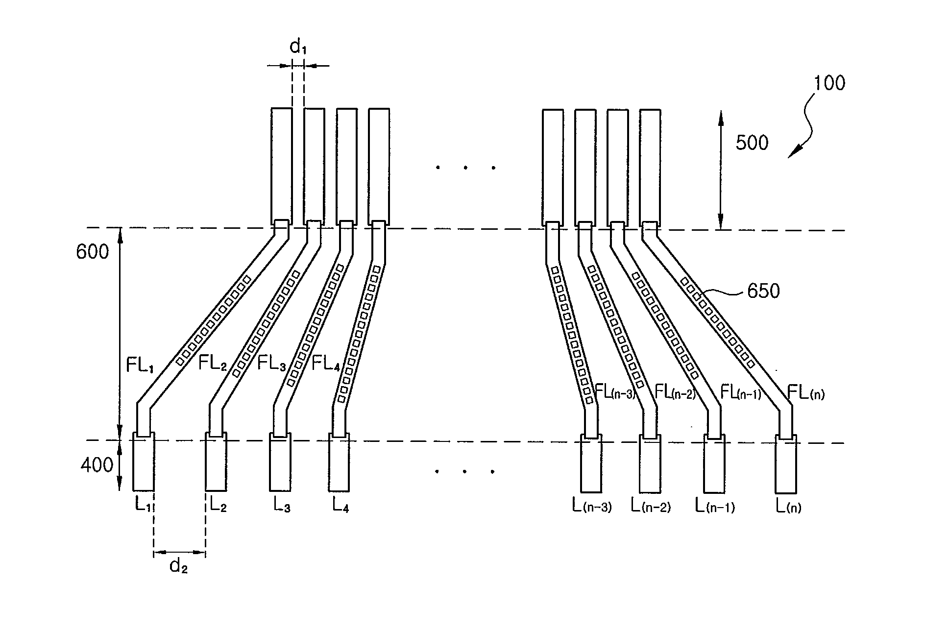
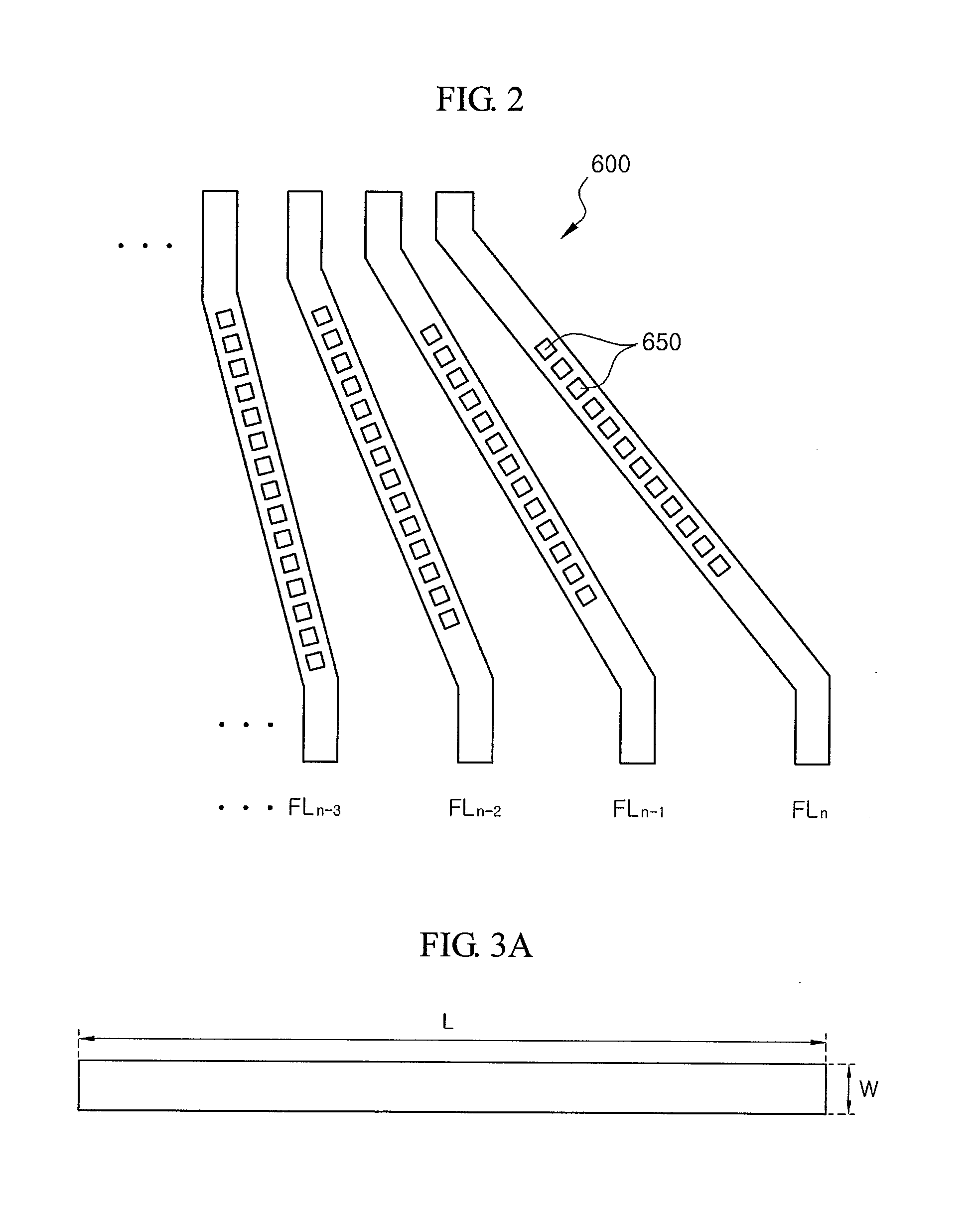
[0025]FIG. 1 is a plan view schematically illustrating a fanout line part according to an embodiment of the present invention, and FIG. 2 is an enlarged view of a portion of the fanout line part illustrated in FIG. 1. A fanout line part 600 according to the embodiment illustrated in FIGS. 1 and 2 includes fanout lines having different lengths and the same width. FIG. 2 illustrates the N-3rd fanout line FLn-3 to the Nth fanout line FLn.

[0026]With reference to FIG. 1, signal lines 400, bonding pads 500, and the fanout line part 600 are formed on a substrate 100 of the flat display panel. The fanout line part 600 is formed between the signal lines 400 and the bonding pads 500 to electrically connect the signal lines 400 and...


PUM

PropertyMeasurementUnit
structureaaaaaaaaaa
lengthsaaaaaaaaaa
resistanceaaaaaaaaaa

Abstract

A fanout line structure and a liquid crystal display panel and a liquid crystal display including the fanout line structure are presented. The fanout line structure connects a signal line to a bonding pad, and includes a plurality of fanout lines that are positioned apart from each other. The plurality of fanout lines are formed to have different lengths, and a hole pattern is formed in at least one of the plurality of fanout lines to reduce the difference in resistance levels between the fanout lines. The fanout structure significantly reduces any deterioration in image quality stemming from different resistance levels among the fanout lines.

Description

CROSS-REFERENCE TO RELATED APPLICATION[0001]This application claims priority from Korean Patent Application No. 2006-0125732 filed on Dec. 11, 2006, the disclosure of which is incorporated by reference in its entirety.BACKGROUND OF THE INVENTION[0002]1. Field of the Invention[0003]The present invention relates generally to a fanout line structure usable in a liquid crystal display and, more particularly, to a fanout line structure that is capable of ensuring equivalent resistance.[0004]2. Description of the Related Art[0005]Possible applications for liquid crystal displays (LCDs) expand as progress is made in their weight reduction, thickness reduction, power consumption reduction, full-color display capability, and resolution improvement. In a liquid crystal display, the amount of light that is transmitted is controlled according to the image signal that is applied to a plurality of control switches arranged in a matrix configuration. By activating the switches selectively, desired...

Claims


Application Information

Patent Timeline
Patent Type & Authority Applications(United States)
IPC IPC(8): G02F1/1343H03K19/0175
CPCG02F1/13452G02F1/1345
Inventor KIM, SO WOONYANG, SUNG HOONCHAI, CHONG CHUL
Owner SAMSUNG DISPLAY CO LTD
Why Eureka
Try Eureka