Laterally Interconnected IC Packages and Methods

a technology of lateral interconnection and ic package, which is applied in the direction of printed circuit, sustainable manufacturing/processing, final product manufacturing, etc., can solve the problems of reducing the area required on the substrate, the inability to increase density while reducing the area, and the inability to meet the practical limit, so as to achieve faster data throughput, reduce costs, and increase the pin count of the package

Inactive Publication Date: 2008-07-03
TEXAS INSTR INC
View PDF5 Cites 0 Cited by
  • Summary
  • Abstract
  • Description
  • Claims
  • Application Information

AI Technical Summary

Benefits of technology

[0010]The invention has numerous advantages including but not limited to providing methods and devices offering one or more of the following; smaller package footprints, higher pin count packages for given footprints, faster data throughput, and reduced costs. These and other features, advantages, and benefits of the present invention can be understood by one of ordinary skill in the arts upon careful consideration of the detailed description of representative embodiments of the invention in connection with the accompanying drawings.

Problems solved by technology

Efforts are continuously underway to design and manufacture devices with reduced area, but attempts to increase density while reducing area must inevitably reach a practical limit.
One notable disadvantage of this type of arrangement is the area required on the substrate.

Method used


Image

  • Laterally Interconnected IC Packages and Methods
  • Laterally Interconnected IC Packages and Methods
  • Laterally Interconnected IC Packages and Methods

Examples


Embodiment Construction

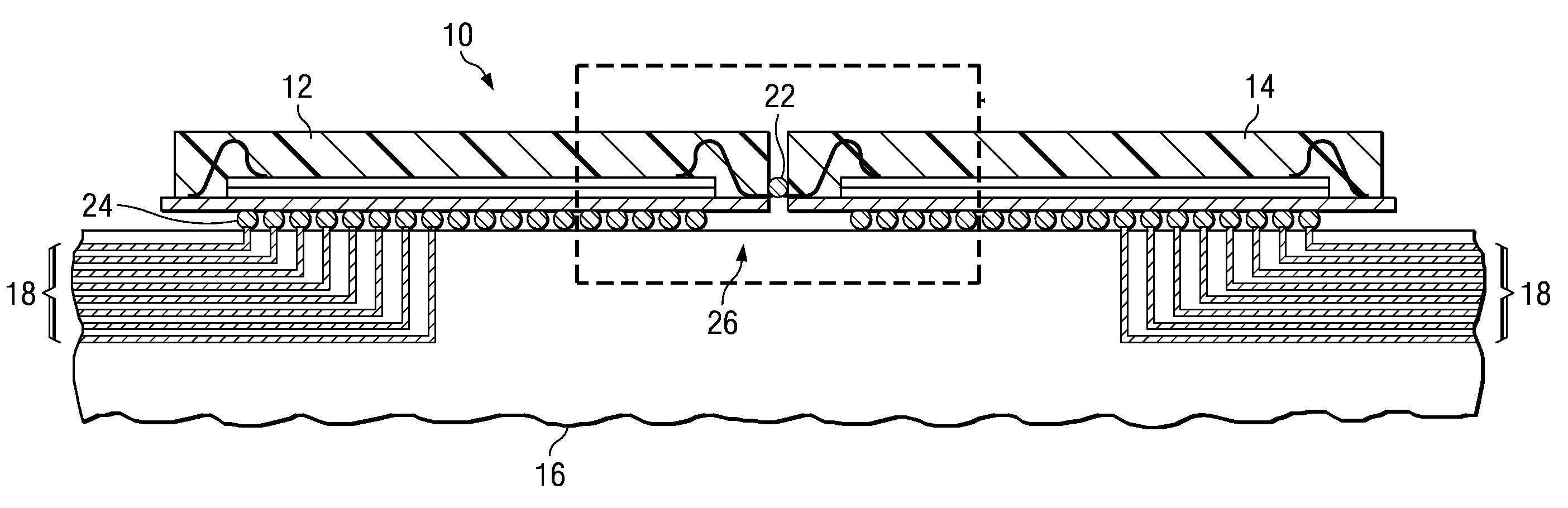
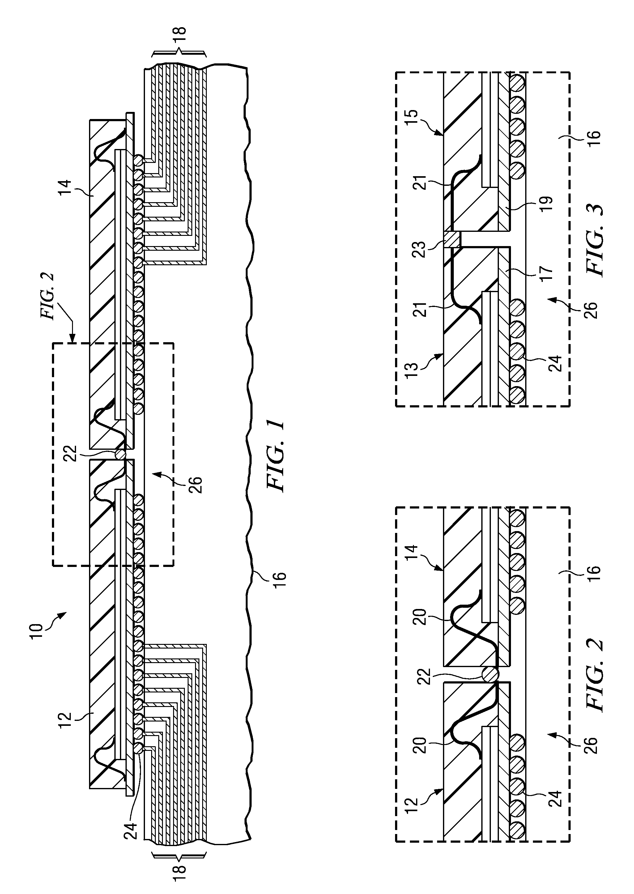
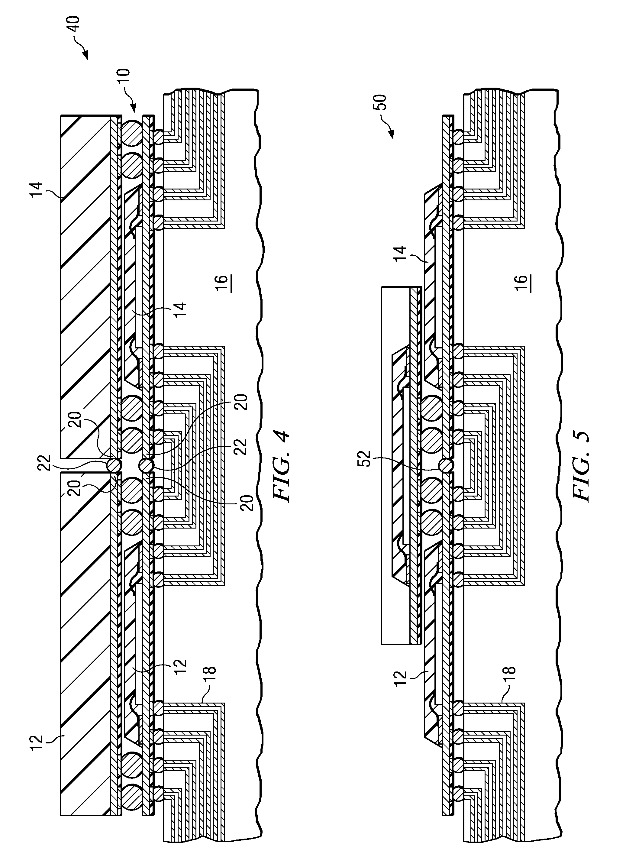
[0018]In general, the invention provides improvements in multi-package semiconductor device assemblies. Laterally interconnected multi-IC configurations facilitate direct communication of electronic signals among adjacent semiconductor devices with decreased reliance on a board interface.

[0019]Now referring primarily to FIG. 1, an example of preferred embodiments of the invention are shown. A multi-package semiconductor device system 10 has a first packaged semiconductor device 12 and a second packaged semiconductor device 14. The first and second devices 12, 14, are adjacent to one another in a coplanar configuration, preferably affixed on a substrate 16, in this case a PCB, although other suitable substrates may be used, such as a PWB, or in the context of a PoP system, another packaged device or coplanar grouping of packaged devices. The substrate 16 typically includes subsurface metallic traces 18 within. The first device 12, and the second device 14, each have at least one late...


PUM


Abstract

Semiconductor devices and methods for their assembly are described in which IC packages may be combined in novel configurations. A multi-package semiconductor device system and associated methods for its construction include a plurality of packaged semiconductor devices, each provided with at least one lateral electrical contact. The plurality of packaged semiconductor devices so provided are fixed in a coplanar configuration and have the adjacent lateral contacts coupled for operation in concert.

Description

TECHNICAL FIELD[0001]The invention relates to electronic semiconductor devices and manufacturing. More particularly, the invention relates to microelectronic semiconductor devices and their packages and to methods and systems for implementing assemblies having lateral interconnections among IC packages.BACKGROUND OF THE INVENTION[0002]Semiconductor device assemblies are subject to many competing design goals. It is very often desirable to minimize the size of electronic apparatus. At the same time, the demand for increased features results in an increase in the number of components on a given device. Efforts are continuously underway to design and manufacture devices with reduced area, but attempts to increase density while reducing area must inevitably reach a practical limit.[0003]In lateral multi-device layouts, semiconductor devices are placed on a planar substrate such as a PCB or PWB. Typically, electrical connections are made between each device and the substrate by coupling ...

Claims


Application Information

Patent Timeline
Patent Type & Authority Applications(United States)
IPC IPC(8): H01L23/48H01L21/58
CPCH01L23/3128H01L2924/01033H01L24/49H01L25/105H01L2224/32225H01L2224/4809H01L2224/48091H01L2224/48175H01L2224/48227H01L2224/49H01L2224/73265H01L2924/014H01L2924/14H01L2924/15192H01L2924/15311H01L2924/15331H05K1/112H05K1/181H05K2201/09227H05K2201/09627H05K2201/1053H05K2201/10734H01L24/48H01L2225/1005H01L2225/1058H01L2225/1023H01L2924/00014H01L2924/00H01L2924/00012H01L24/73H01L2224/48472H01L2924/181Y02P70/50H01L2224/45099H01L2224/05599
Inventor HARRISON, RAY D.ZHU, JIANBAIWOLFE, JEFFREY J.STEPNIAK, FRANK
Owner TEXAS INSTR INC
Why Eureka
Try Eureka