Pipelined semiconductor memories and systems

a technology of semiconductor memories and systems, applied in the field of electronic systems, can solve the problems of not being able to address pipelining in general, address pipelining in particular, bank/block/sector/row/subarray, etc., and achieve the effects of low cost, low power consumption, and fast data throughpu

Active Publication Date: 2007-08-07
S AQUA SEMICONDUCTOR LLC
View PDF23 Cites 104 Cited by
  • Summary
  • Abstract
  • Description
  • Claims
  • Application Information

AI Technical Summary

Benefits of technology

[0005]All of the above memories without an exception, desire fast data throughput at low cost and low power. Although data pipelining and prefetching from the memory core have been described in prior art, address pipelining in general, bank / block / sector / row / subarray and address pipelining in particular, have not been attempted. It is one embodiment of the invention to pipeline all addresses at the same rate as data, independent of the address function (row, column, bank, block, sector). It is another embodiment of the invention to pipeline those addresses on both the rising and falling edges of SCLK (System clock) or a primary clock for that particular system or IC. It is yet another purpose and embodiment of the invention to provide a global command and control supervisory circuitry for each monolithic integrated circuit that optimizes the efficiency of a multi bank / block / sector IC. The word “bank” is used here, synonymously with block, sector, subarray etc. It is also another embodiment to pipeline addresses at a rate faster than data, or, even slower than data in an asynchronous manner.
[0006]Although preferred embodiments are described in this invention, the implementation and extension of the principles of the invention are not limited. For those skilled in the art, the principles described in this invention will be obvious. The principles of the present invention are embodied in memory system architectures and operating methods utilizing multiple banks (blocks, sectors, subarrays) and independent row / column address decoding pipeline. A memory is disclosed where a plurality of independently addressable banks for storing data can function with a decoding pipeline of n-stages where n is greater than 1, and at least 2. The “unit” is one system or primary clock (SCLK, CLK) period. Row and column addresses can be continuously pipelined from the address input parts. Global address supervisory circuitry allows a sequence of addresses to be continuously received, and, properly implemented, without conflict at any stage.

Problems solved by technology

Although data pipelining and prefetching from the memory core have been described in prior art, address pipelining in general, bank / block / sector / row / subarray and address pipelining in particular, have not been attempted.

Method used


Image

  • Pipelined semiconductor memories and systems
  • Pipelined semiconductor memories and systems
  • Pipelined semiconductor memories and systems

Examples


Embodiment Construction

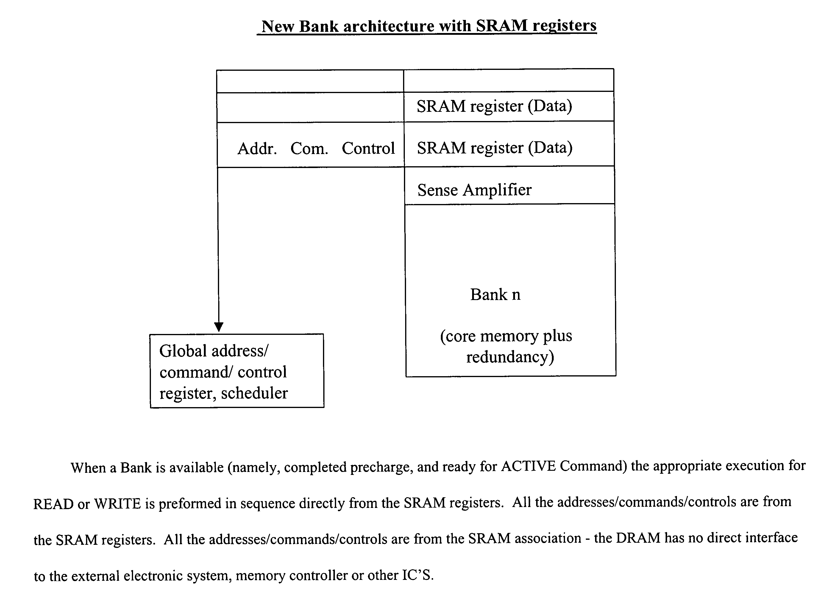
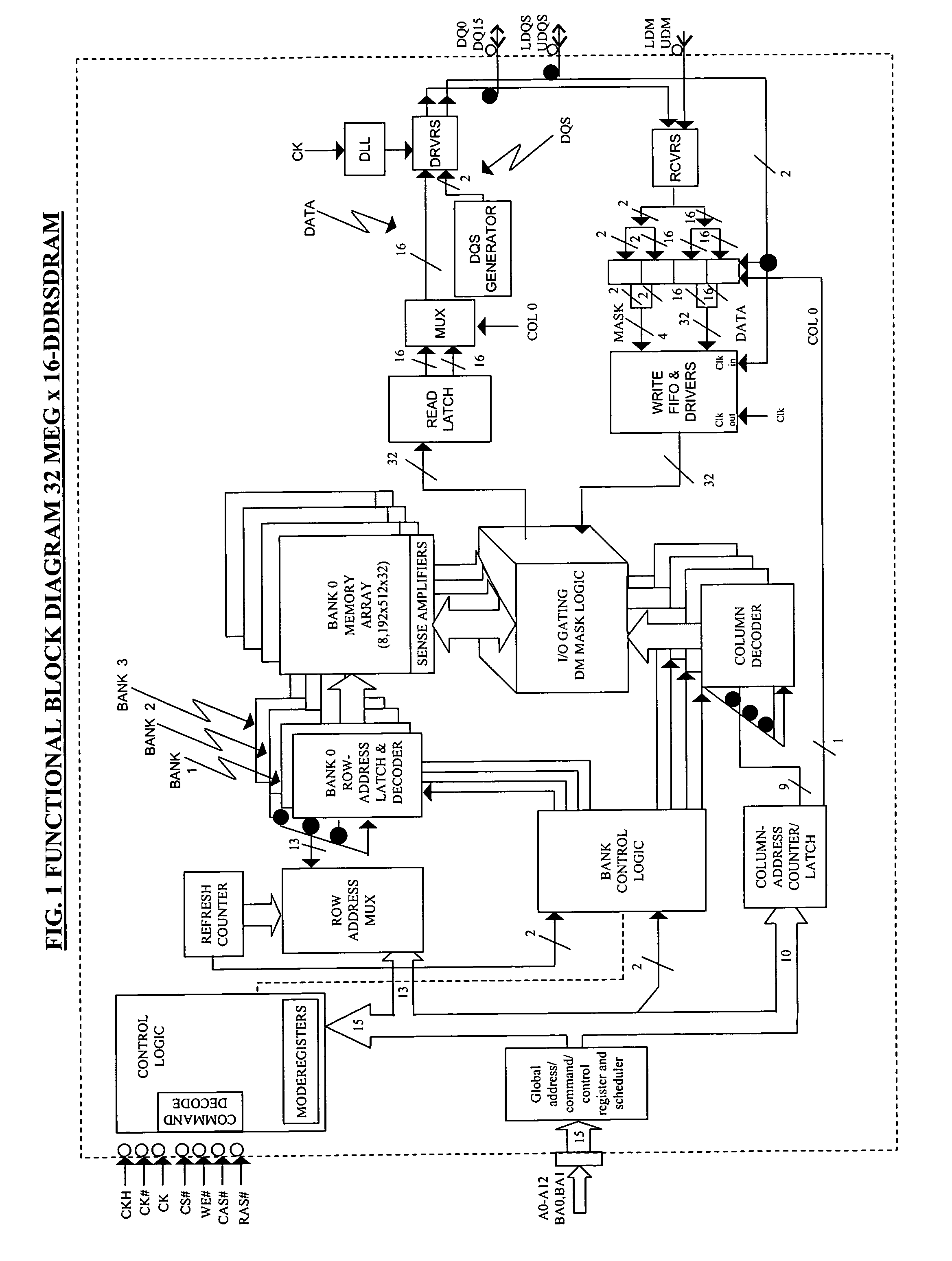
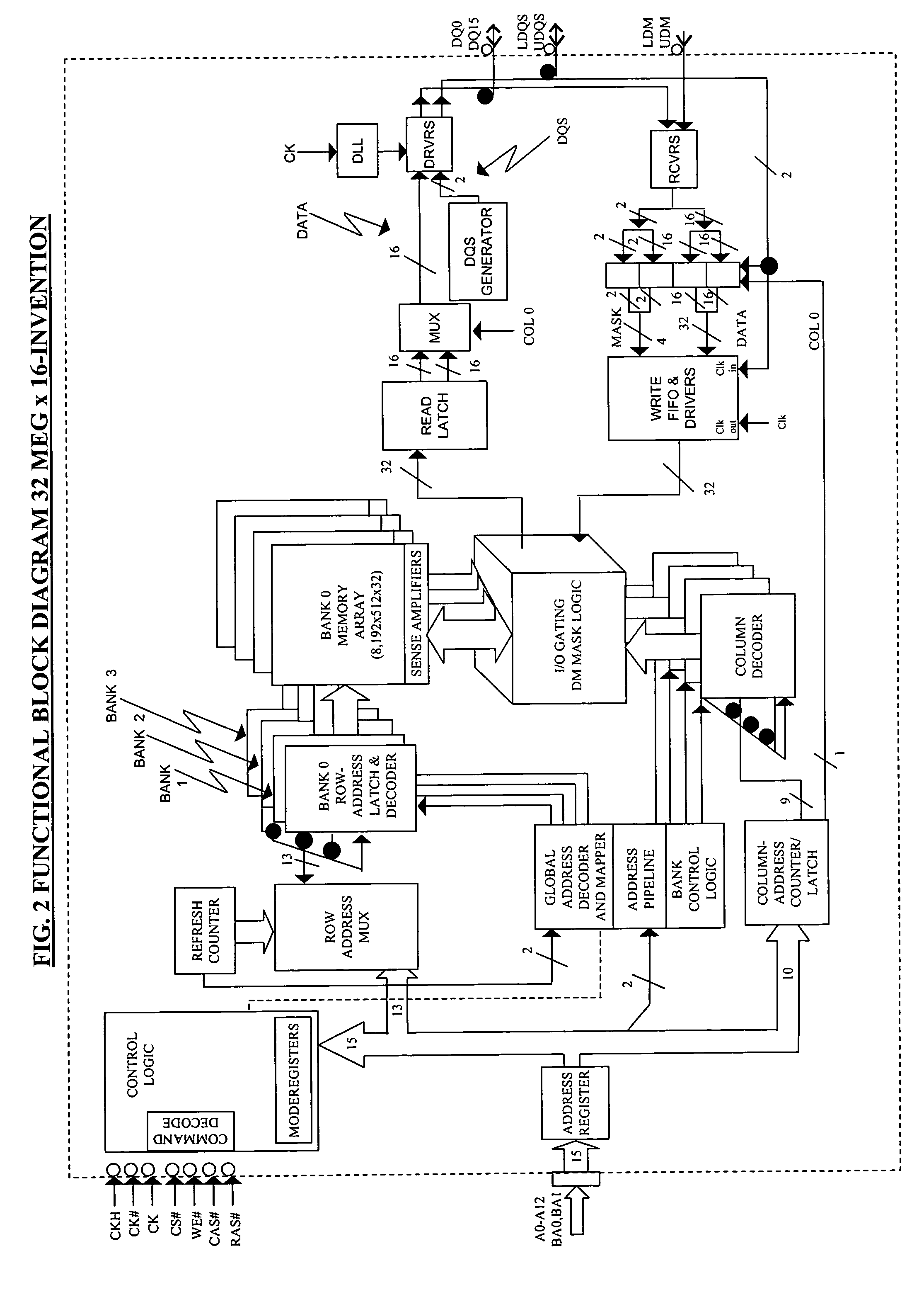
[0011]The principles of the present invention and their advantages are best understood by referring to the illustrated embodiments depicted in FIGS. 1-4 of the drawings, in which like numbers designate like parts. The inventions described below apply to any memory, namely, DRAM, SRAM, EPROM, EEPROM, Flash, Mag RAM, FeRAM, PCRAM, plastic RAM, CNTRAM, Molecular RAM etc. The inventions apply to both non-multiplexed address as well as multiplexed-address integrated circuits. The inventions described below apply to what is known in the industry as “row” chain—namely, selecting block / bank / sector / subarray / row in any IC (integrated circuit) or system (consisting of several IC's) or SOC (System On Chip). The inventions apply to single-ended or rail-to-rail address / data / clock signals. The inventions apply to the “column” chain as well. The inventions apply to “data bursts”, “prefetch schemes”, “page schemes” and similar architectures known in the industry. The effective bandwidth of a device ...


PUM


Abstract

The invention describes and provides pipelining of addresses to memory products. Addresses are pipelined to multibank memories on both rising and falling edges of a clock. Global Address Supervisor pipelines these addresses optimally without causing bank or block or subarray operational conflicts. Enhanced data through put and bandwidth, as well as substantially improved bus utilization (simultaneously), can be realized. In peer-to-peer connected systems, significant random data access throughput can be obtained.

Description

CROSS-REFERENCE TO RELATED APPLICATION[0001]The Patent Application claims priority to provisional patent Application Ser. No. 60 / 475,224 entitled “Pipelined Semiconductor Memories” filed Jun. 2, 2003 by inventor G. R. Mohan Rao.FIELD OF INVENTION[0002]The present invention relates in general to electronic systems comprising semiconductor integrated circuits. It relates in particular to pipelined memories in standalone (discrete) as well as embedded (system-on-chip, system-in-package) implementations.BACKGROUND OF THE INVENTION[0003]Peak data bandwidth, average data bandwidth, fast bus turnaround, maximum bus utilization and efficiency, low power, nonvolatility—all at an affordable cost—are key requirements for semiconductor components. Specifically, for semiconductor memories, there are additional requirements as well. For example, balanced read / write operational efficiency in communication systems, is necessary. In some systems dominated by ‘page’ architectures (DRAM, Flash are som...

Claims


Application Information

Patent Timeline
Patent Type & Authority Patents(United States)
IPC IPC(8): G06F12/00G11C7/10
CPCG11C7/1039
Inventor RAO, G.R. MOHAN
Owner S AQUA SEMICONDUCTOR LLC
Why Eureka
Try Eureka