IC package and method of manufacturing the same

a technology of integrated circuits and packaging, which is applied in the direction of printed circuit aspects, sustainable manufacturing/processing, final product manufacturing, etc., can solve the problems of low reliability of ic packages, high functionality and speed of ic packages, and requires plenty of time and cost to manufacture, so as to prevent stress

Inactive Publication Date: 2008-07-03
SAMSUNG ELECTRONICS CO LTD
View PDF6 Cites 36 Cited by
  • Summary
  • Abstract
  • Description
  • Claims
  • Application Information

AI Technical Summary

Benefits of technology

[0014]The present general inventive concept provides an IC package including a plurality of BGA IC packages mounted as a stack on a printed circuit board wherein the diameter of solder balls of the upp

Problems solved by technology

In order to accomplish high functionality and speed of mobile products using a single IC package, however, the development of such an IC package with suc

Method used


Image

  • IC package and method of manufacturing the same
  • IC package and method of manufacturing the same
  • IC package and method of manufacturing the same

Examples


Embodiment Construction

[0031]Reference will now be made in detail to the embodiment of the present general inventive concept, examples of which are illustrated in the accompanying drawings, wherein like reference numerals refer to like elements throughout. The embodiment is described below to explain the present general inventive concept by referring to the figures.

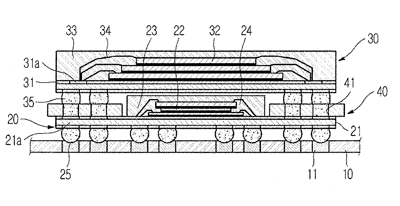
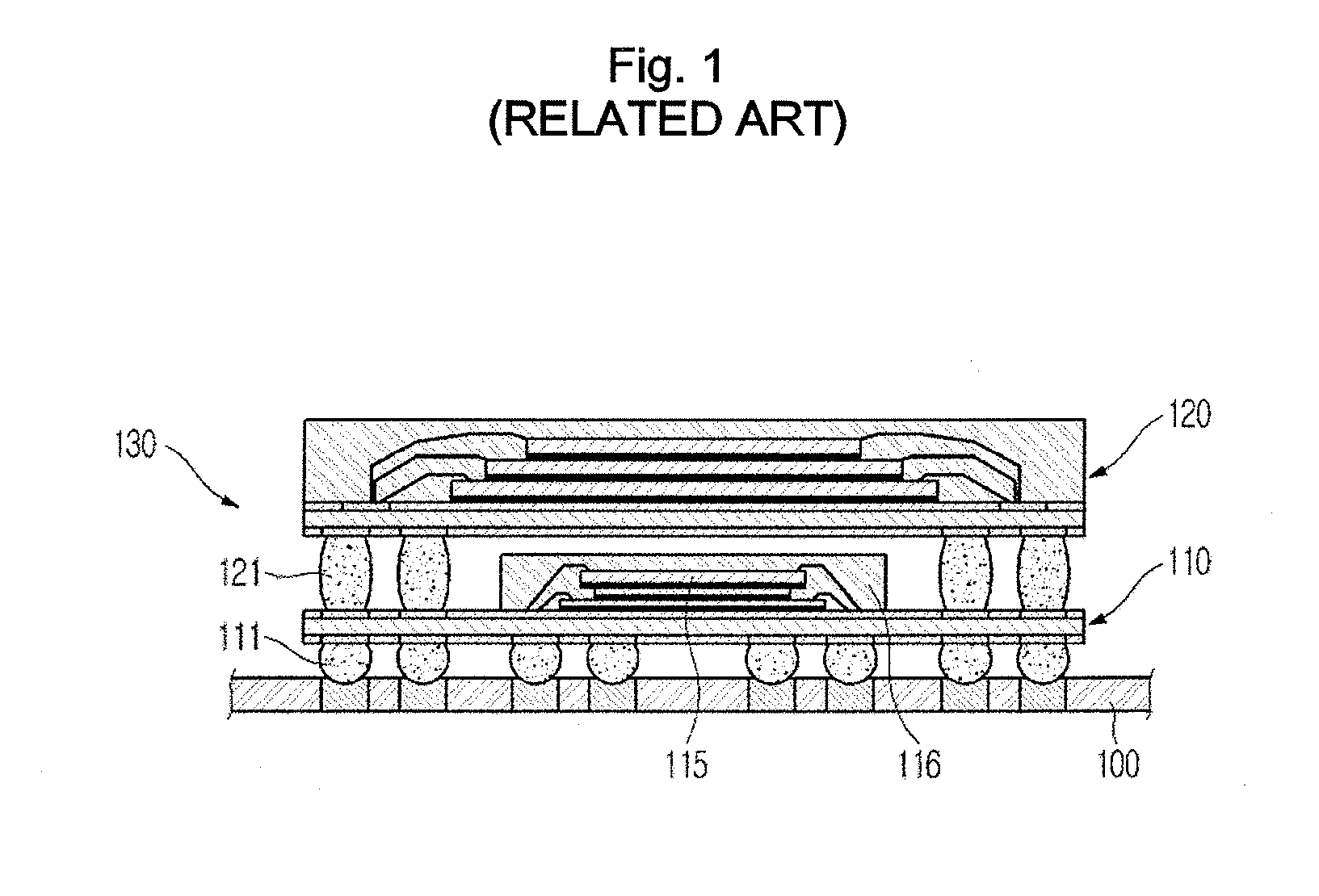
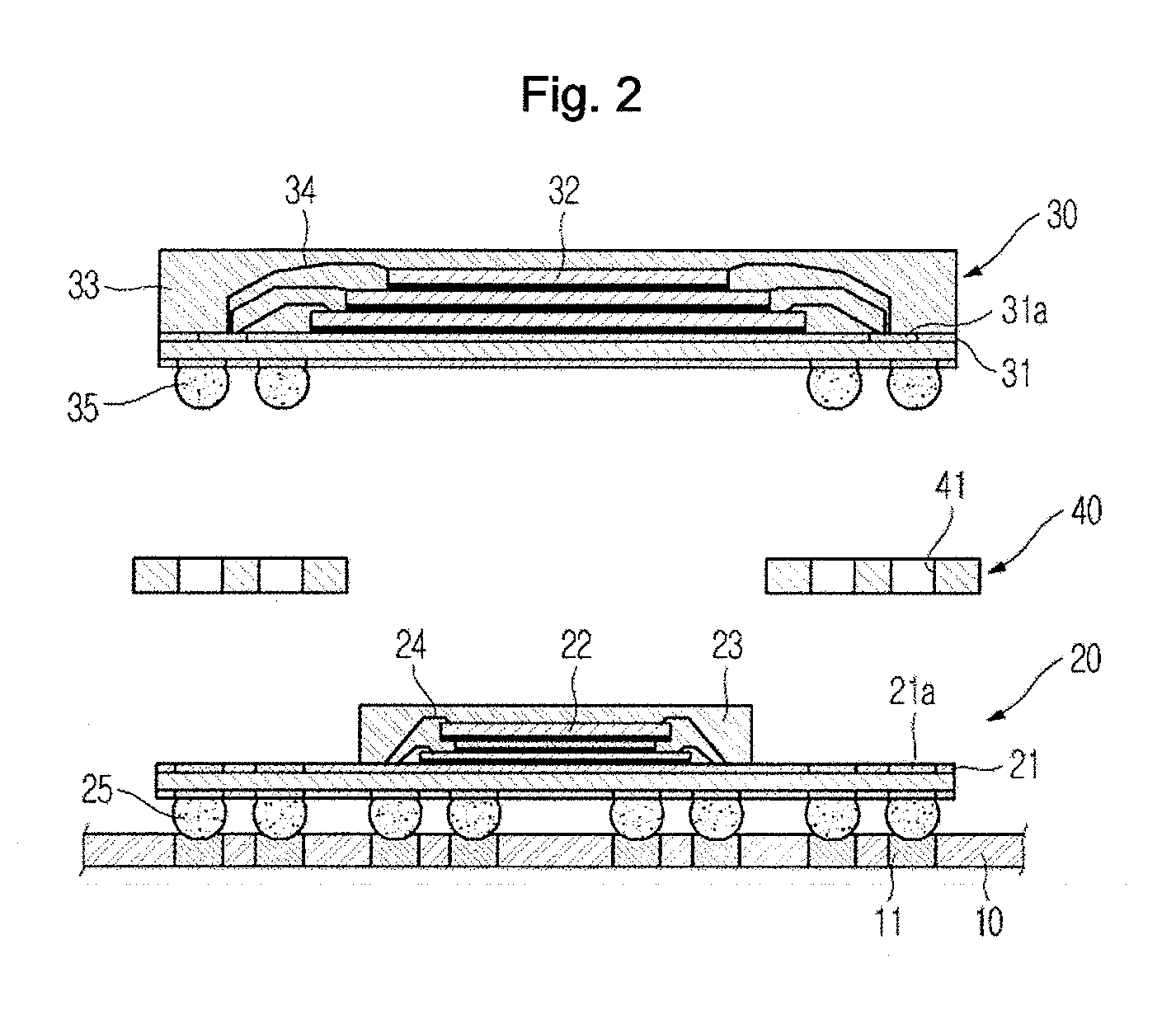
[0032]As illustrated in FIG. 2, an IC package according to an embodiment of the present general inventive concept includes a printed circuit board 10, a first BGA IC package 20 joined to a top portion of the printed circuit board 10, a second BGA IC package 30 stacked on the first BGA IC package 20, and an interposer 40 interposed between the first BGA IC package 20 and the second BGA IC package 30.

[0033]On the printed circuit board 10 is formed a circuit pattern 11, which is circuitly connected to the first and second BGA IC packages 20 and 30.

[0034]The first and second BGA IC packages 20 and 30 respectively include printed circuit boards 21 a...


PUM


Abstract

An IC package including a plurality of BGA IC packages stacked on a printed circuit board and a method of manufacturing the same. The IC package includes a printed circuit board, a first BGA IC package, having a plurality of first solder balls, stacked on the printed circuit board, a second BGA IC package, having a plurality of second solder balls, stacked on the first BGA IC package, and an interposer having a plurality of through-holes, which are filled by the second solder balls in a molten state such that the length of the second solder balls increases while the second solder balls harden, the interposer being joined to the top of the first BGA IC package.

Description

CROSS-REFERENCE TO RELATED APPLICATIONS[0001]This application claims the benefit of Korean Patent Application No. 2007-000675, filed on Jan. 3, 2007 in the Korean Intellectual Property Office, the disclosure of which is incorporated herein by reference in its entirety.BACKGROUND OF THE INVENTION[0002]1. Field of the Invention[0003]The present general inventive concept relates to an integrated circuit (IC) package including a plurality of ball grid array (BGA) IC packages stacked on a printed circuit board (PCB), and a method of manufacturing the same.[0004]2. Description of the Related Art[0005]Recently, mobile products, such as mobile phones, personal digital assistants (PDA), and portable multimedia players, have gradually decreased in weight and size. At the same time, the functionality and speed of the mobile products have increased.[0006]In order to accomplish high functionality and speed of mobile products using a single IC package, however, the development of such an IC packa...

Claims


Application Information

Patent Timeline
IPC IPC(8): H01L23/538H01L21/60
CPCH01L23/3128H01L2225/1023H01L2224/48227H01L2224/73265H01L2225/0651H01L2225/06575H05K3/3436H05K2201/10378H05K2201/10424H05K2201/10515H01L2224/32145H01L2224/32225H01L25/105H01L2225/107H01L2924/15311H01L2924/00H01L2924/00012H01L24/73H01L2924/14Y02P70/50H01L23/488
Inventor HAN, HYUN JOOPARK, TAO SANGJANG, SE YEONGMOON, YOUNG JUNKIM, JUNG HYEONKANG, SUNG WOOK
Owner SAMSUNG ELECTRONICS CO LTD
Why Eureka
Try Eureka