Surface Inspection Method and Surface Inspection Apparatus

a surface inspection and apparatus technology, applied in the direction of instruments, measurement devices, scientific instruments, etc., can solve the problems of low anisotropy of background scattered light in angular directions, low contribution rate of background scattered light to the total quantity, etc., to reduce the contribution rate of output signal with high noise level, and judge the noise level of output signal

Active Publication Date: 2008-07-24
HITACHI HIGH-TECH CORP
View PDF4 Cites 16 Cited by
  • Summary
  • Abstract
  • Description
  • Claims
  • Application Information

AI Technical Summary

Benefits of technology

[0014]To solve the above problem, in the surface inspection in accordance with the present invention, light that is scattered, diffracted or reflected on a surface of an object to be inspected or in the vicinity of the surface is detected by use of a plurality of photodetectors in a plurality of directions, and weighted addition processing or weighted averaging processing by a linear combination of a plurality of signals obtained thereby is performed, whereby a contaminant particle and a defect on the surface of the object to be inspected and the like are detected. The size of the contaminant particle and the defect is calculated from results of the weighted addition processing or weighted averaging processing. Incidentally, the weighted addition processing or the weighted averaging processing is performed so that among output signals from the plurality of photodetectors, the contribution rate of an output signal with a high noise level decreases. In order to judge the noise level of output signals from each photodetector, outputs signals from each photodetector are divided into signals for at least two systems: a first divided output signal and a second divided output signal, and signal processing is performed in such a manner that a first signal component corresponding to the intensity of light generated by deriving from the roughness of the surface of the object to be inspected, which belongs to the light scattered, diffracted or reflected from the surface of the object to be inspected or in the vicinity of the surface, is taken out of the first divided output signal, and a second signal component corresponding to the intensity of light generated by deriving from a contaminant particle and a defect on the surface of the object to be inspected or in the vicinity of the surface, which belongs to the light scattered, diffracted or reflected from the surface of the object to be inspected or in the vicinity of the surface, is taken out of the second divided output signal. It is advisable to use a low-pass filter to take out the first signal component, and to use a band-pass filter to take out the second signal component.

Problems solved by technology

However, this poses a problem when the relative ratio of background scattered light to the total quantity of scattered light and the anisotropy of background scattered light in angular directions are not very large as described above.

Method used


Image

  • Surface Inspection Method and Surface Inspection Apparatus
  • Surface Inspection Method and Surface Inspection Apparatus
  • Surface Inspection Method and Surface Inspection Apparatus

Examples


Embodiment Construction

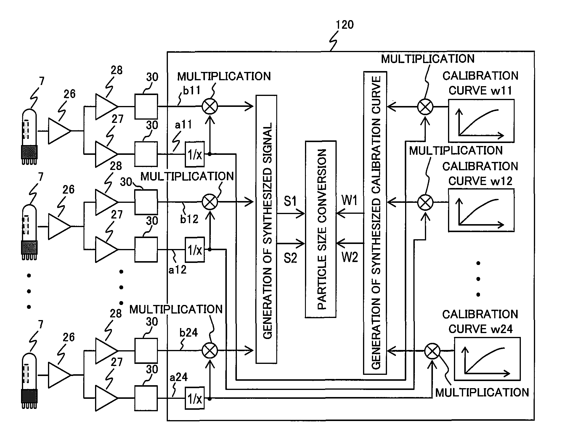
[0032]As described above, the present invention provides a surface inspection method and a surface inspection apparatus that are capable of detecting scattered light from a contaminant particle and a defect at a good S / N even when the relative ratio of background scattered light to the total quantity of scattered light and the anisotropy of background scattered light in angular directions are not relatively large in a case where background scattered light deriving from the surface roughness of a semiconductor wafer has directivity in the direction of an elevation angle or an azimuthal angle and in a case where the directivity of background scattered light changes depending on positions on a wafer to be inspected. Particularly, when, for example, a surface inspection technique for detecting scattered light by use of a plurality of photodetectors is used in a plurality of directions in which a plurality of elevation angles and a plurality of azimuthal angles are combined, the present ...


PUM

PropertyMeasurementUnit
azimuthal anglesaaaaaaaaaa
anglesaaaaaaaaaa

Abstract

Provided are a surface inspection method and a surface inspection apparatus that are capable of detecting scattered light from a contaminant particle and a defect at a good S/N even when the relative ratio of background scattered light to the total quantity of scattered light and the anisotropy of background scattered light in angular directions are not relatively large in a case where background scattered light deriving from the surface roughness of a semiconductor wafer has directivity in a direction of an elevation angle or an azimuthal angle and in a case where the directivity of background scattered light changes depending on positions on a wafer to be inspected. In surface inspection according to the present invention, by use of a plurality of photodetectors arranged in a plurality of directions, light scattered, diffracted or reflected on a surface of an object to be inspected or in the vicinity of the surface is detected and a plurality of signals obtained by this are subjected to weighted addition processing or weighted averaging processing by linear combination, whereby a contaminant particle and a defect on a surface of an object to be inspected and the like are detected. The size of a contaminant particle and a defect is calculated from results of the weighted addition processing or weighted averaging processing.

Description

BACKGROUND OF THE INVENTION[0001]1. Field of the Invention[0002]The present invention relates to a surface inspection method and a surface inspection apparatus that are intended for detecting micro contaminant particles and defects present on a semiconductor substrate (a semiconductor wafer).[0003]2. Background Art[0004]In production lines of semiconductor substrates (semiconductor wafers), contaminant particles adhering to the substrate surface and defects, such as scratches occurring during processing, are inspected in order to monitor the dust generating condition of the manufacturing equipment. For example, in a semiconductor substrate before the formation of circuit patters, it is necessary to detect micro contaminant particles and defects on the surface to the nearest several tens of nanometers or less. In the above-described inspection of the substrate surface, crystal defects present in a shallow region near the substrate surface and the surface roughness of the substrate su...

Claims


Application Information

Patent Timeline
Patent Type & Authority Applications(United States)
IPC IPC(8): G01N21/00
CPCG01N21/9501G01N21/4738
Inventor MATSUI, SHIGERU
Owner HITACHI HIGH-TECH CORP
Why Eureka
Try Eureka