
Method of sorting dies using discrimination region

Inactive Publication Date: 2008-08-07
SAMSUNG ELECTRONICS CO LTD
View PDF3 Cites 9 Cited by
  • Summary
  • Abstract
  • Description
  • Claims
  • Application Information

AI Technical Summary

Benefits of technology

[0009]Also, the present invention provides a method of enabling efficient correspondence between a wafer map and an actual wafer.

Problems solved by technology

In general, all of the dies do not operate properly due to variations in the fabrication process.
When the sorting process is not properly performed, bad dies may be packaged, while good dies may be discarded.
However, for a wafer with small thickness and large area, the inking method may damage the wafer, and so, the ink method has recently been replaced by an inkless sorting method.
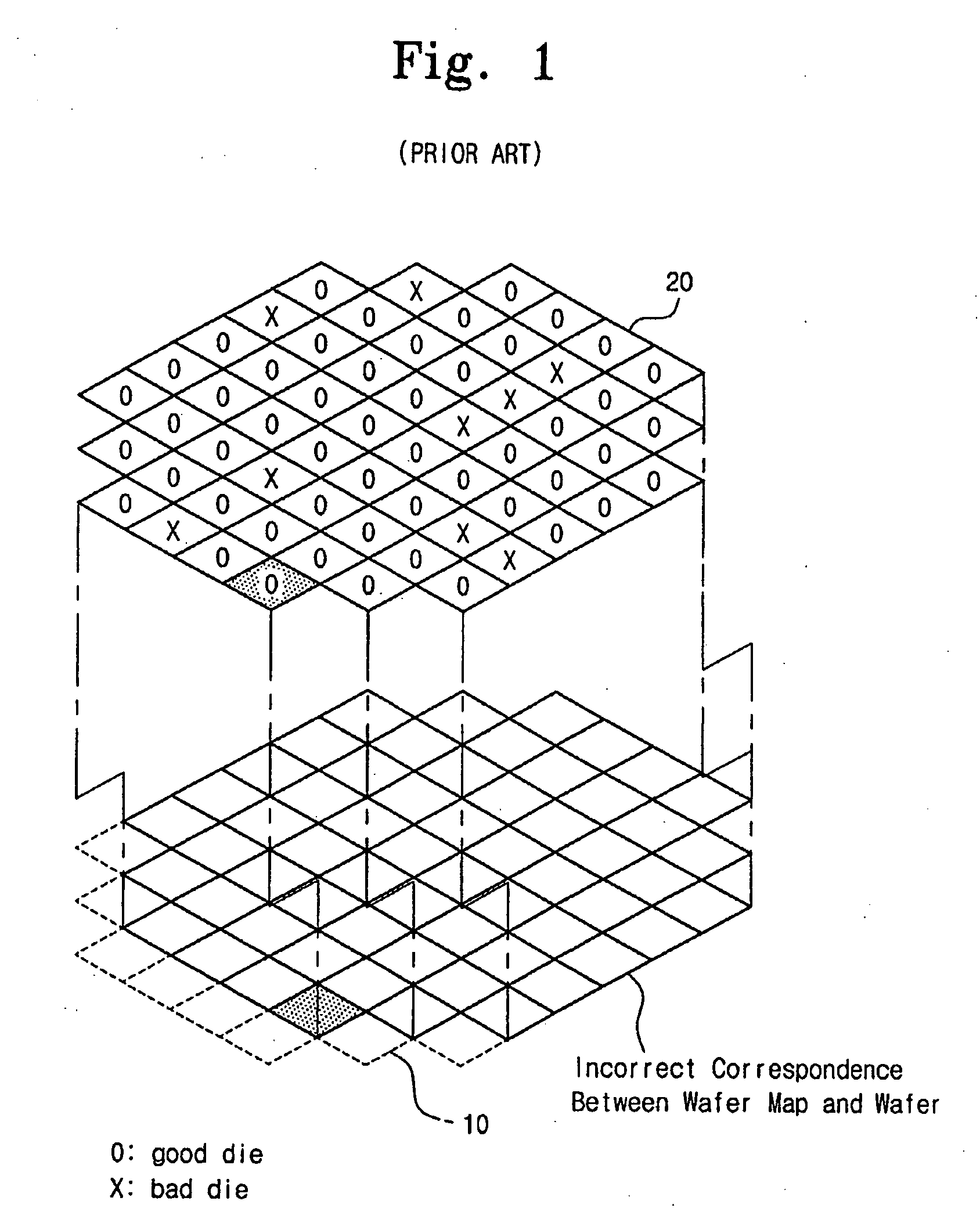
However, since the packaging process is performed at a different time, i.e., in a different process step, and in a different place, i.e., in a different system, from the electrical test, for a wafer having a plurality of dies, there is still a possibility of incorrect correspondence between a wafer map 20 and an actual wafer 10 as illustrated in FIG. 1.
This incorrect correspondence can be caused by operator error.

Method used


Image

  • Method of sorting dies using discrimination region
  • Method of sorting dies using discrimination region
  • Method of sorting dies using discrimination region

Examples


Embodiment Construction

[0025]Reference will now be made in detail to the preferred embodiments of the present invention, examples of which are illustrated in the accompanying drawings.

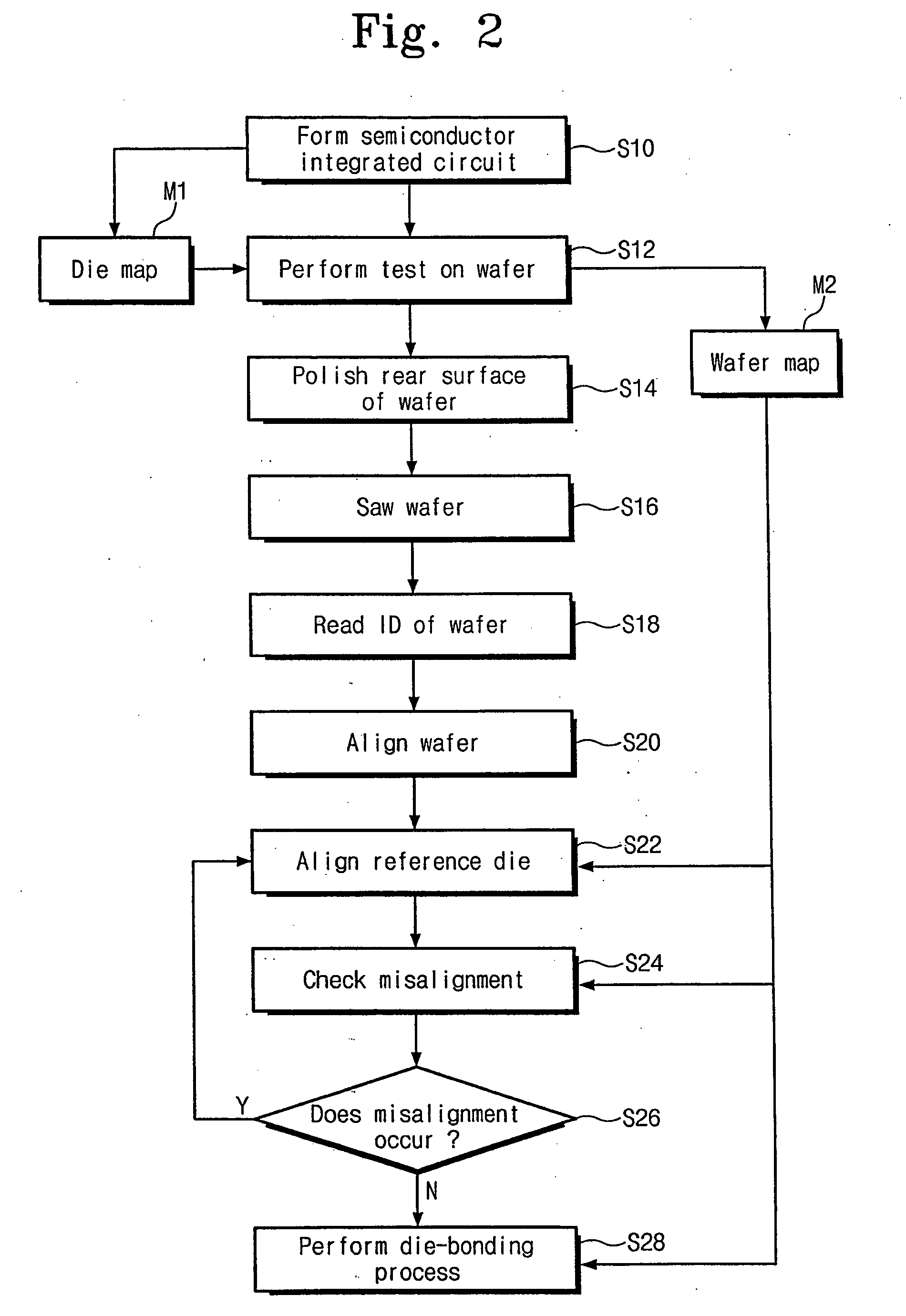
[0026]It will be understood that when a layer is referred to as being “on” another layer or substrate, it can be directly on the other layer or substrate, or intervening layers may also be present. In the drawings, the thicknesses of layers and regions are exaggerated for clarity. It will be understood that although the terms first and second are used herein to describe various regions, layers and / or sections should not be limited by these terms. These terms are only used to distinguish one region, layer or section from another region, layer or section. Thus, for example, a first layer discussed below could be termed a first layer without departing from the teachings of the present invention. Each embodiment described and illustrated herein includes complementary embodiments thereof FIG. 2 is a process flowchart illustrating...


PUM


Abstract

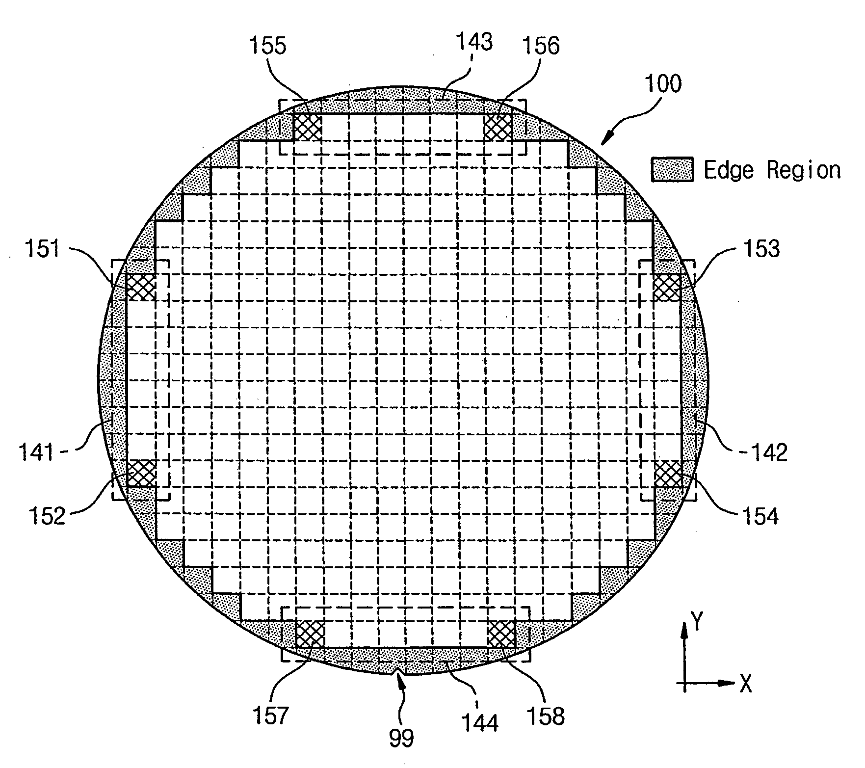
A method of sorting dies using a discrimination region includes preparing a wafer including a chip region in which a plurality of dies are disposed and an edge region in which at least one discrimination region is disposed; testing the dies to prepare a wafer map for defining the coordinates of good dies and bad dies; allowing dies defined by the wafer map to correspond to the dies of the wafer; and confirming the correctness of the correspondence between the wafer and the wafer map by checking whether the discrimination region is included in the dies defined by the wafer map.

Description

[0001]This application claims priority to Korean Patent Application No. 10-2007-0011090, filed in the Korean Intellectual Property Office on Feb. 2, 2007, the entire contents of which are hereby incorporated herein by reference.BACKGROUND OF THE INVENTION[0002]1. Field of the Invention[0003]The present invention relates to a method of fabricating a semiconductor device, and more particularly, to a method of sorting dies using a discrimination region.[0004]2. Description of the Related Art[0005]A semiconductor device is fabricated using a wafer with a plurality of dies. The dies are separated using a wafer sawing process and undergo a packaging process to fabricate individual semiconductor chips. In general, all of the dies do not operate properly due to variations in the fabrication process. Therefore, it is necessary to sort normally operating dies (hereinafter, “good” dies), that is, distinguish good dies from abnormally operating (hereinafter, “bad”) dies. A process of sorting th...

Claims


Application Information

Patent Timeline
IPC IPC(8): H01L21/66
CPCH01L22/20H01L22/00
Inventor KIM, YOUNG-DAEKIM, YUN-KIBAE, SUNG-UN
Owner SAMSUNG ELECTRONICS CO LTD
Learn More