Reference clock receiver compliant with LVPECL, LVDS and PCI-Express supporting both AC coupling and DC coupling

a clock receiver and reference clock technology, applied in the direction of pulse generators, logic circuit coupling/interface arrangements, pulse techniques, etc., can solve the problems that the conventional structure cannot meet the specifications of certain new industry standards, and achieve the effect of boosting the pair of differential outputs

Inactive Publication Date: 2008-08-21
ALTERA CORP
View PDF27 Cites 11 Cited by
  • Summary
  • Abstract
  • Description
  • Claims
  • Application Information

AI Technical Summary

Problems solved by technology

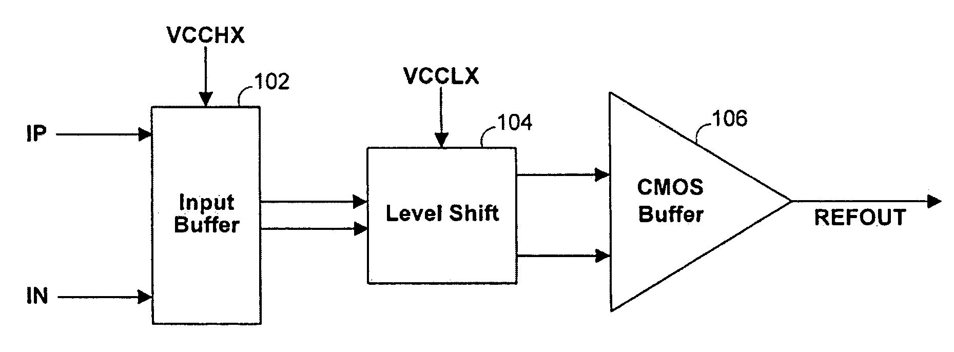
This conventional structure may not be able to meet specifications of certain new industry standards such as PCI-Express, whose reference clocks have a common-mode range from 0.25 volts to 0.55 volts.

Method used


Image

  • Reference clock receiver compliant with LVPECL, LVDS and PCI-Express supporting both AC coupling and DC coupling
  • Reference clock receiver compliant with LVPECL, LVDS and PCI-Express supporting both AC coupling and DC coupling
  • Reference clock receiver compliant with LVPECL, LVDS and PCI-Express supporting both AC coupling and DC coupling

Examples


Embodiment Construction

[0021]FIG. 3 shows a reference clock receiver 300 according to the invention. Reference clock receiver 300 preferably includes three stages: input buffer 301, level shifter 303 and differential-to-single ended converter 305.

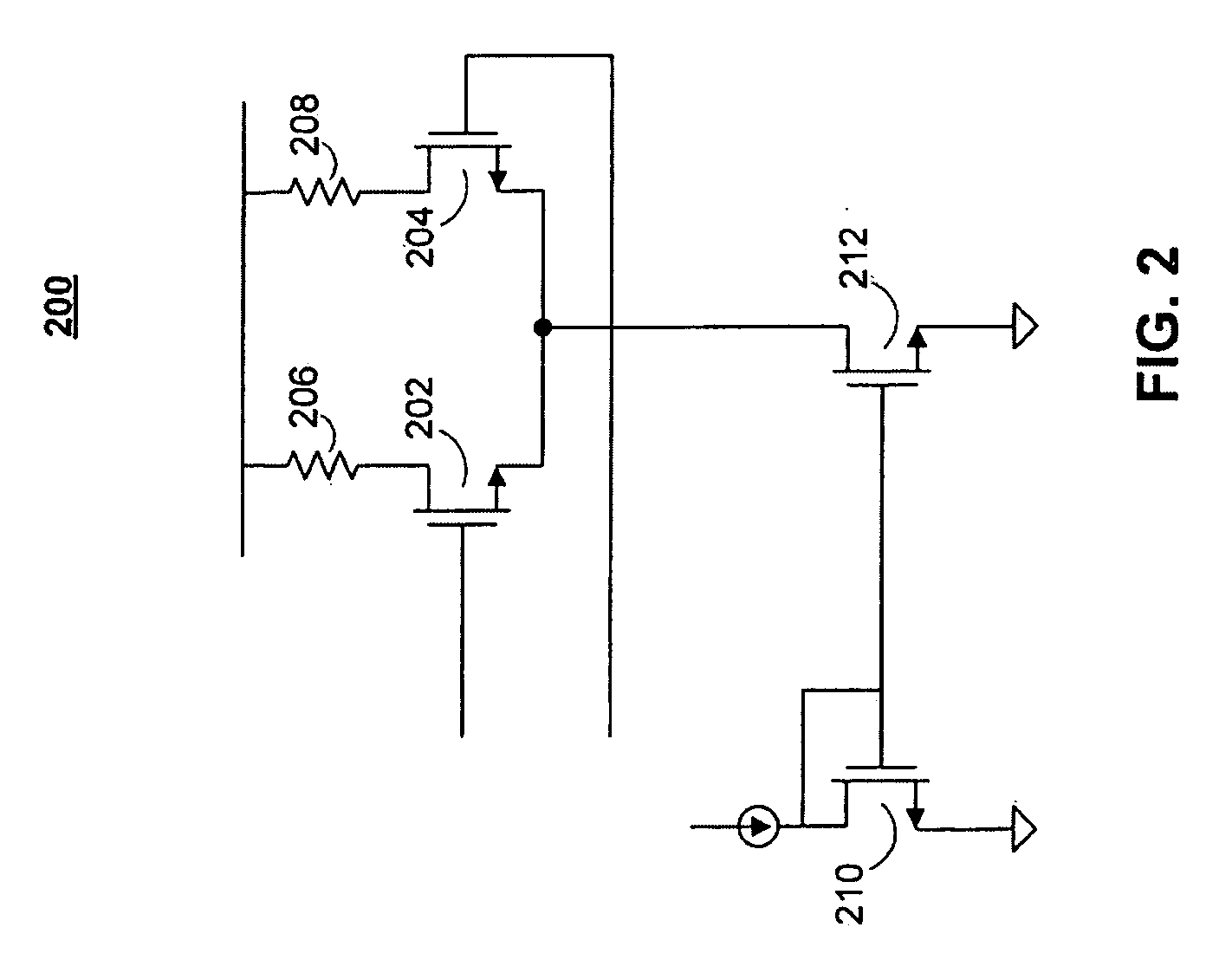
[0022]Input buffer 301 preferably is formed from a PMOS-based differential pair of transistors 308 and 310 (together with resistors 310 and 312 and current mirror transistors 306 and 308) as opposed to the NMOS-based differential pair. By using a supply voltage VCCH=3.3 volts, the input common-mode range can go from about 0 volts to about 2.2 volts. This range is able to cover the voltage common-mode specifications of many industry standards such as PCI-Express (Vcm=0.25V˜0.55V), LVPECL (Vcm=1.8825V˜2.05V) and LVDS (Vcm=1.25 volts).

[0023]Receiver 300 preferably converts relatively high voltage levels to a core voltage level (1.2 volts). Because of this function, receiver 300 preferably uses thick oxide transistors 302, 304, 306 and 308. Thick oxide transistors ar...


PUM


Abstract

A reference clock receiver structure according to the invention is provided. The structure preferably includes an input buffer that is formed from a PMOS differentiated pair of transistors and a first supply voltage. The PMOS differential pair receives a pair of differential inputs, and produces a pair of differential outputs. The structure also includes a level shifter that is coupled to receive the pair of differential outputs from the input buffer to provide gain to the pair of differential outputs to form a gained pair of differential outputs. The level shifter that includes a second supply voltage. The second supply voltage may have a smaller magnitude than the first supply voltage. Finally, the structure includes a CMOS buffer that is coupled to receive the gained pair of differential outputs. The CMOS buffer boosts the gained pair of differential outputs and converts the gained differential pair outputs into a single signal.

Description

BACKGROUND OF THE INVENTION[0001]This invention relates to reference clock receivers for use with Programmable Logic Devices (PCDs) or any other suitable electronic device.[0002]Clock multiplier phase-lock loops (PLL) in transceivers usually require a “clean” reference clock that is generated from an external crystal clock source. The output voltages of the crystal are typically differential voltages. These voltages may be compliant with different standards such as LVPECL (Vcm=1.8825 volts˜2.05 volts), LVDS (Vcm=˜1.25 v volts), and PCI-Express (Vcm=0.25 volts˜0.55 volts). Then a reference clock receiver is needed to take the differential signals with differential voltage levels and convert them to a signal level that is compatible with the core supply voltage in the high-speed serial interface portion of the PLD.[0003]FIG. 1 shows a circuit that shows a conventional reference clock receiver structure 100. Reference clock receiver structure 100 includes input buffer 102, level shift ...

Claims


Application Information

Patent Timeline
Patent Type & Authority Applications(United States)
IPC IPC(8): H03L5/00
CPCH03K3/35613H04L25/0294H04L25/0272
Inventor MEI, HAITAOWANG, SHOUJUNBEREZA, WILLIAM W.BAIG, MIRZA M.
Owner ALTERA CORP
Why Eureka
Try Eureka