Non-volatile semiconductor memory using charge-accumulation insulating film
Active Publication Date: 2008-09-11
KIOXIA CORP
View PDF5 Cites 17 Cited by
- Summary
- Abstract
- Description
- Claims
- Application Information
AI Technical Summary
Benefits of technology
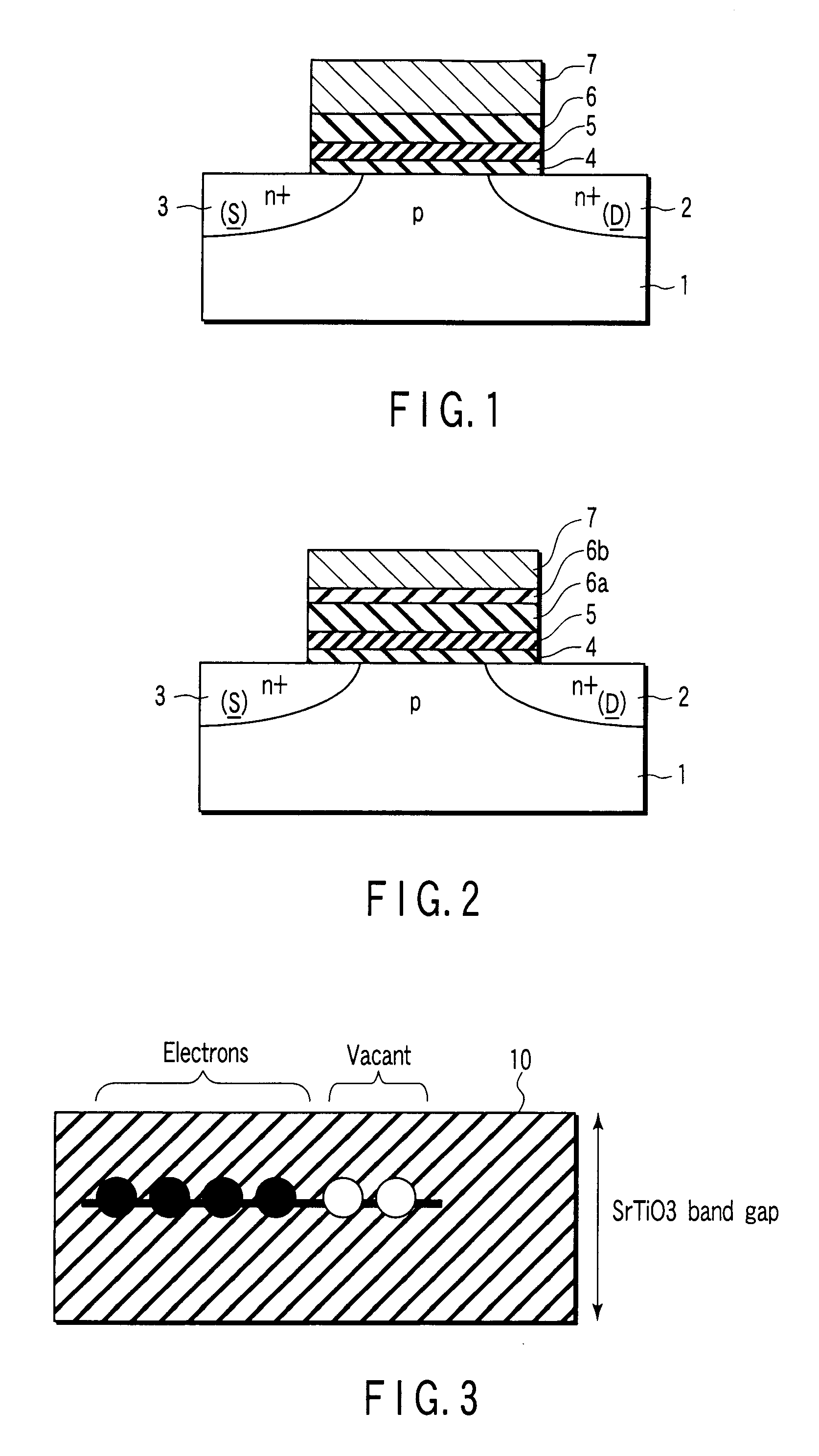
[0014]wherein the gate multilayer material is obtained by sequentially stacking: a first insulating layer that is formed on the channel region; a charge accumulation layer that is formed of an oxide dielectric material in which at least one of Tc, Re, Ru, Os, Rh, Ir, Pd, Pt, Co, Ni, W, Mo, Cr, Mn, and Fe as a substance having a higher valence than titanium (Ti), zirconium (Zr), and hafnium (Hf) is introduced as an additive substance and which includes at least one of Ti, Zr, and Hf; a second insulating layer having a dielectric constant higher than the first insulating layer; and a memory gate electrode.
[0015]Further, the non-volatile semiconductor memory includes: a semiconductor substrate having a source region and a drain region provided therein to form a gap serving as a channel region therebetween; and a gate multilayer material that has both ends provided on the source region and the drain region and is formed on the channel region, and the gate multilayer material is constituted by sequentially stacking: a first insulating layer formed on the channel region; a charge accumulation layer in which at least one of Tc, Re, Ru, Os, Rh, Ir, Pd, Pt, Co, and Ni as substances having valences higher than titanium (Ti), zirconium (Zr), or hafnium (Hf) is introduced as an additive substance into an oxide dielectric film including at least one of Ti, Zr, and Hf in such a manner that an area density falls within a range of 1×10¹² to 2×1014 cm−2; a second insulating layer having a dielectric constant higher than the first insulating layer; and a memory gate electrode.
[0016]Furthermore, the non-volatile semiconductor memory includes: a semiconductor substrate having a source region and a drain region provided therein to form a gap serving as a channel
Problems solved by technology
In a NAND flash memory in the next and subsequent generations requiring miniaturization and a low-voltage operation, realization of a flat cell is demanded because of a difficulty in embedding inter-poly-dielectrics (IPD) in a space between cells.
In case of an FG structure in which electric charges are accumulated in a metal gate film, when a local defect occurs in the tunnel film, a great part of accumulated charges is lost through this defect.
Although the above-explained MONOS has a structure in which electric charges are accumulated in a silicon nitride (SiN), an amount of charge accumulation is insufficient, and there is a problem that a large threshold voltage variation range cannot be assured.
When an ingenuity, e.g., increasing an amount of silicon is exercised to increase the amount of charge accumulation, a metallic state is obtained, and the same problem as that in the conventional FG
Method used
View moreImage
Smart ImageViewing Examples

Examples
 PUM
 Abstract
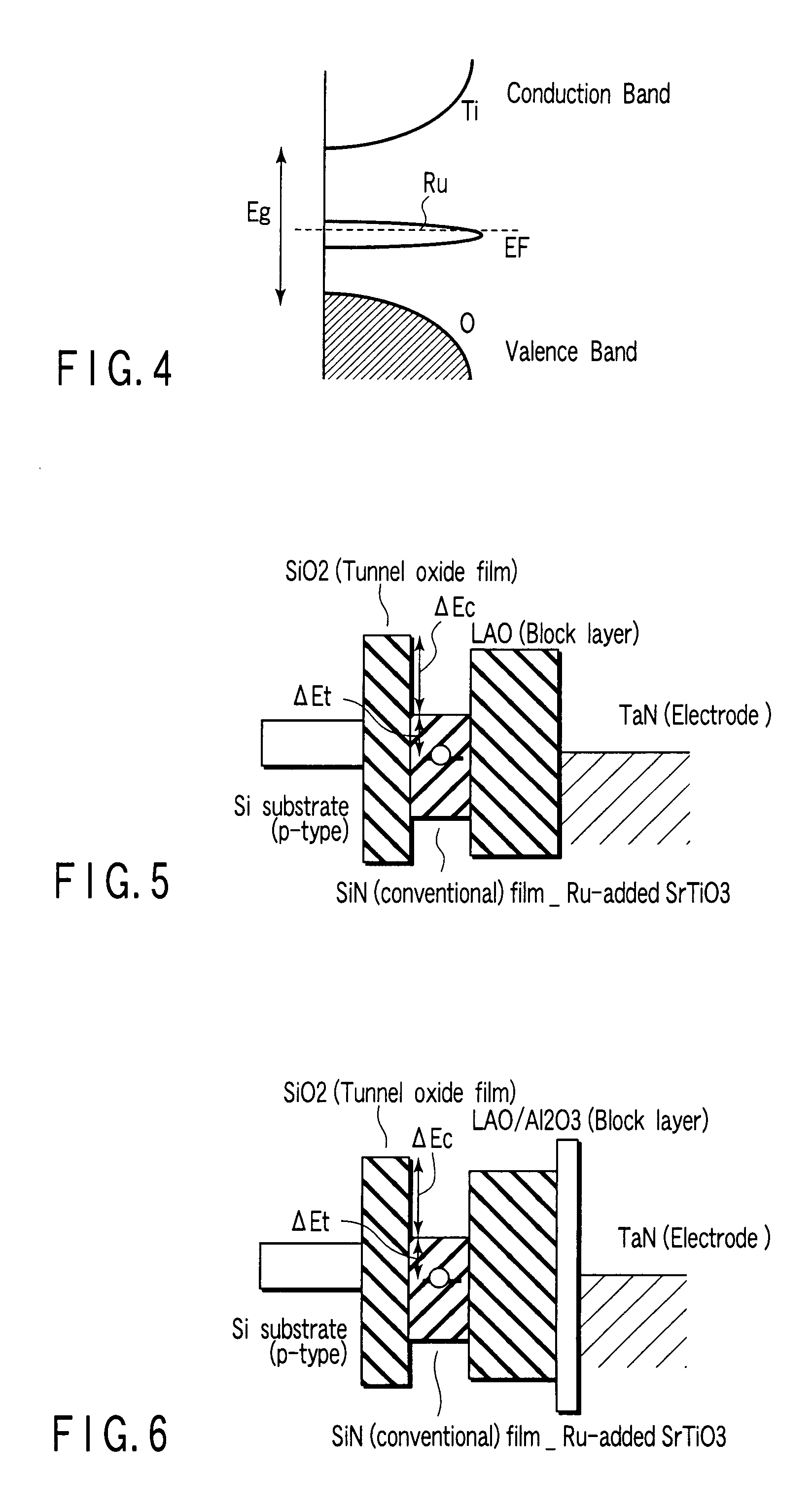
There is provided a non-volatile semiconductor memory having a charge accumulation layer of a configuration where a metal oxide with a dielectric constant sufficiently higher than a silicon nitride, e.g., a Ti oxide, a Zr oxide, or a Hf oxide, is used as a base material and an appropriate amount of a high-valence substance whose valence is increased two levels or more (a VI-valence) is added to produce a trap level that enables entrance and exit of electrons with respect to the base material.
Description
CROSS-REFERENCE TO RELATED APPLICATIONS[0001]This application is based upon and claims the benefit of priority from prior Japanese Patent Application No. 2006-267983, filed Sep. 29, 2006, the entire contents of which are incorporated herein by reference.BACKGROUND OF THE INVENTION[0002]1. Field of the Invention[0003]The present invention relates to a non-volatile semiconductor memory using a charge-accumulation insulating film formed by introducing a high-valence substance into a high-dielectric material made of an oxide.[0004]2. Description of the Related Art[0005]In general, a flash memory that is one of non-volatile semiconductor memories is a non-volatile memory that does not require an electrical holding operation (holding power supply) for accumulation, and it is often used in electronic devices since a program and others can be readily written even after completion of a product.[0006]In a NAND flash memory in the next and subsequent generations requiring miniaturization and a...
Claims
Login to View More Application Information
Patent Timeline
 IPC IPC(8): H01L29/792
CPCH01L27/115H01L27/11568H01L29/792H01L29/513H01L29/66833H01L29/4234H10B69/00H10B43/30
Inventor SHIMIZU, TATSUOMURAOKA, KOICHI
Owner KIOXIA CORP
Features
- Generate Ideas
- Intellectual Property
- Life Sciences
- Materials
- Tech Scout
- Unparalleled Data Quality
- Higher Quality Content
- 60% Fewer Hallucinations
Learn More Browse by: Latest US Patents, China's latest patents, Technical Efficacy Thesaurus, Application Domain, Technology Topic, Popular Technical Reports.
© 2025 PatSnap. All rights reserved.Legal|Privacy policy|Modern Slavery Act Transparency Statement|Sitemap|About US| Contact US: help@patsnap.com