Microbatch deposition chamber with radiant heating

a technology of radiant heating and deposition chamber, which is applied in the direction of crystal growth process, polycrystalline material growth, chemically reactive gas growth process, etc., can solve the problems of adversely affecting film properties, poor device performance, and reaction ra

Inactive Publication Date: 2008-09-11
APPLIED MATERIALS INC
View PDF13 Cites 38 Cited by
  • Summary
  • Abstract
  • Description
  • Claims
  • Application Information

AI Technical Summary

Benefits of technology

[0010]The present invention generally provides methods and apparatus for processing semiconductor substrates. In particular, embodiments of the present invention provide a chemical vapor deposition (CVD) epitaxial processing chamber that can process two or more substrates simultaneously while retaining many of the advantages of single substrate processing.

Problems solved by technology

However, lower process temperatures can slow chemical reaction rates which can adversely affect film properties.
In epitaxial films, lack of uniformity can lead to poor device performance.
However, gas flow will still affect thickness.
Unfortunately, a single substrate processing reactor cannot match the throughput of a batch (over 50 substrates), mini-batch (about 25-50 substrates), or micro-batch (less than 25 substrates) LPCVD epitaxial reactor.

Method used


Image

  • Microbatch deposition chamber with radiant heating
  • Microbatch deposition chamber with radiant heating
  • Microbatch deposition chamber with radiant heating

Examples


Embodiment Construction

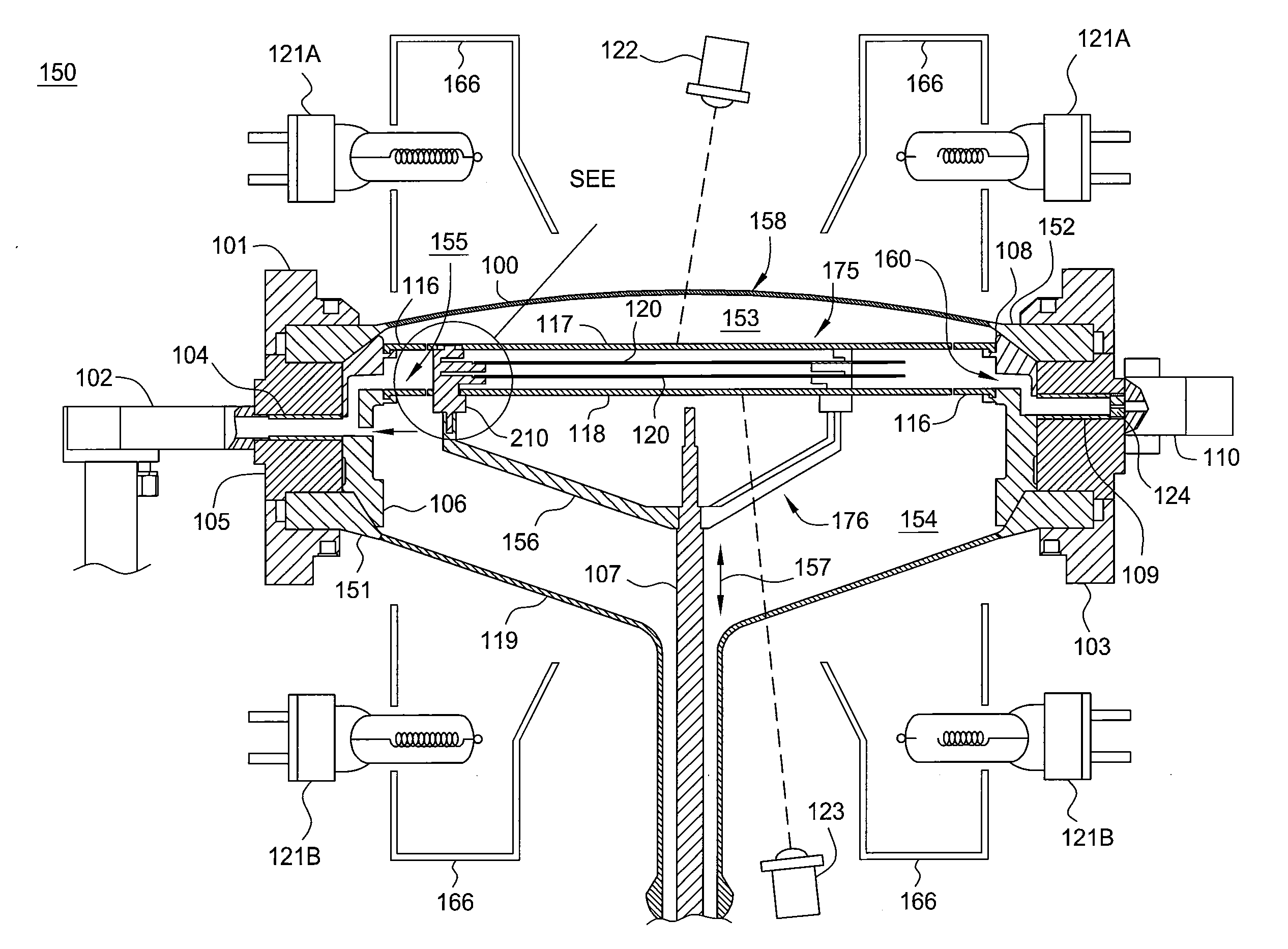
[0035]The present invention generally provides an apparatus and method for an epitaxial deposition chamber that has the capability of processing more than one substrate at a time while retaining the many favorable aspects of single substrate processing. Embodiments of the invention described herein are adapted to maximize uniformity of gas flow and temperature across the surfaces of the substrates and, hence, provide uniformity and repeatability of process results.

[0036]FIG. 1 is a schematic cross-sectional view of an epitaxial deposition reactor chamber 150 according to one embodiment of the present invention. The reactor chamber 150 includes a processing chamber 158 with an enclosed processing volume 175 and high-intensity upper lamps 121A and lower lamps 121B for radiant heating. In the present embodiment, the processing chamber is a cold wall, LPCVD chamber.

[0037]The processing chamber 158 includes an upper dome 100, a lower dome 119, and a base ring 105. The base ring 105 may b...


PUM

PropertyMeasurementUnit
distanceaaaaaaaaaa
temperatureaaaaaaaaaa

Abstract

The present invention generally provides an apparatus and method for processing and transferring substrates in an epitaxial deposition chamber. Embodiments of the invention described herein are adapted to maximize chamber throughput and improve film deposition uniformity. In one embodiment, two substrates are processed simultaneously using radiant heating of the substrates in a cold wall, low pressure chemical vapor deposition reactor.

Description

BACKGROUND OF THE INVENTION[0001]1. Field of the Invention[0002]Embodiments of the present invention generally relate to the deposition of films onto semiconductor substrates, such as silicon wafers. In particular, embodiments of the invention relate to methods and apparatus used in depositing epitaxial films onto semiconductor substrates.[0003]2. Description of the Related Art[0004]The growth of silicon-containing epitaxial films has become increasingly important due to new applications for advanced semiconductor devices. Such films may be grown selectively or non-selectively (blanket deposition) on the substrate. By selective growth it is generally meant that an epitaxial film is grown at specific locations on a substrate having device feature patterns already incorporated therein. For example, the substrate may include patterns for gate electrodes, spacers, ultra-shallow junctions, or other features. To avoid damaging such device features during fabrication, it may be desirable t...

Claims


Application Information

Patent Timeline
Patent Type & Authority Applications(United States)
IPC IPC(8): C23C16/52B05D3/02C23C16/00
CPCC23C16/45591C23C16/4584C30B29/06C30B25/14C30B25/12H01L21/02365
Inventor MERRY, NIRCHANDRASEKHAR, BALASUBRAMANYAM
Owner APPLIED MATERIALS INC
Why Eureka
Try Eureka