
Visual inspection apparatus

a technology of visual inspection and apparatus, which is applied in the direction of measuring devices, instruments, scientific instruments, etc., can solve the problems of chip or crack formation in the peripheral edges of semiconductor wafers, and damage to the wafer during manufactur

Inactive Publication Date: 2008-09-18
OLYMPUS CORP
View PDF5 Cites 14 Cited by
  • Summary
  • Abstract
  • Description
  • Claims
  • Application Information

AI Technical Summary

Benefits of technology

[0008]The present invention provides a visual inspection apparatus for making a visual inspection of a peripheral edge of a wafer pursuant to a preset recipe, the visual inspection apparatus including: a wafer holder that holds a wafer so as to be rotatable; a peripheral edge imaging section that acquires an enlarged image of a peripheral edge of the wafer; an inspection area specifying section that enables the setting of information of an inspection position on the peripheral edge of the wafer at the time of setting a recipe; and a control unit that prepares and registers a recipe for making an inspection of the inspection position set by the inspection area specifying section and that controls the wafer holder and the peripheral edge imaging section to make an inspection pursuant to the registered recipe.

Problems solved by technology

In semiconductor fabrication factories or the like, chips or cracks may be formed in the peripheral edges of semiconductor wafers.
When such defects exist, they may cause damage to a wafer during manufacture.
If a wafer is destroyed, damage occurs such that manufacturing apparatuses must be stopped for a long period of time, etc.
When a measured value of any one image exceeds a threshold value, it is considered that a failure occurs in the removal of resist.

Method used


Image

  • Visual inspection apparatus
  • Visual inspection apparatus
  • Visual inspection apparatus

Examples


first embodiment

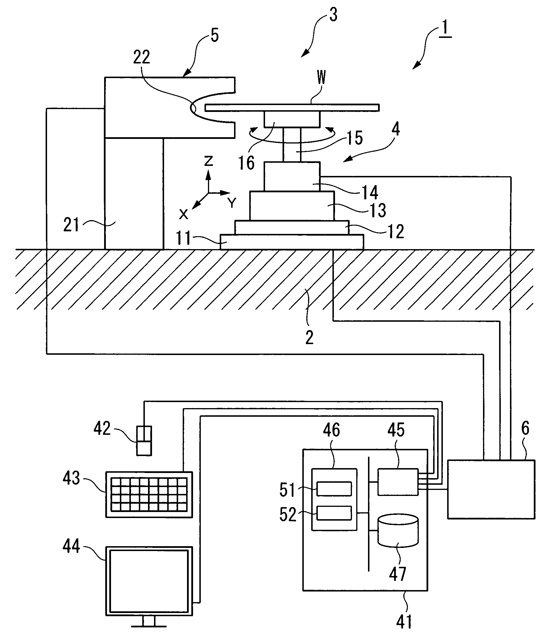
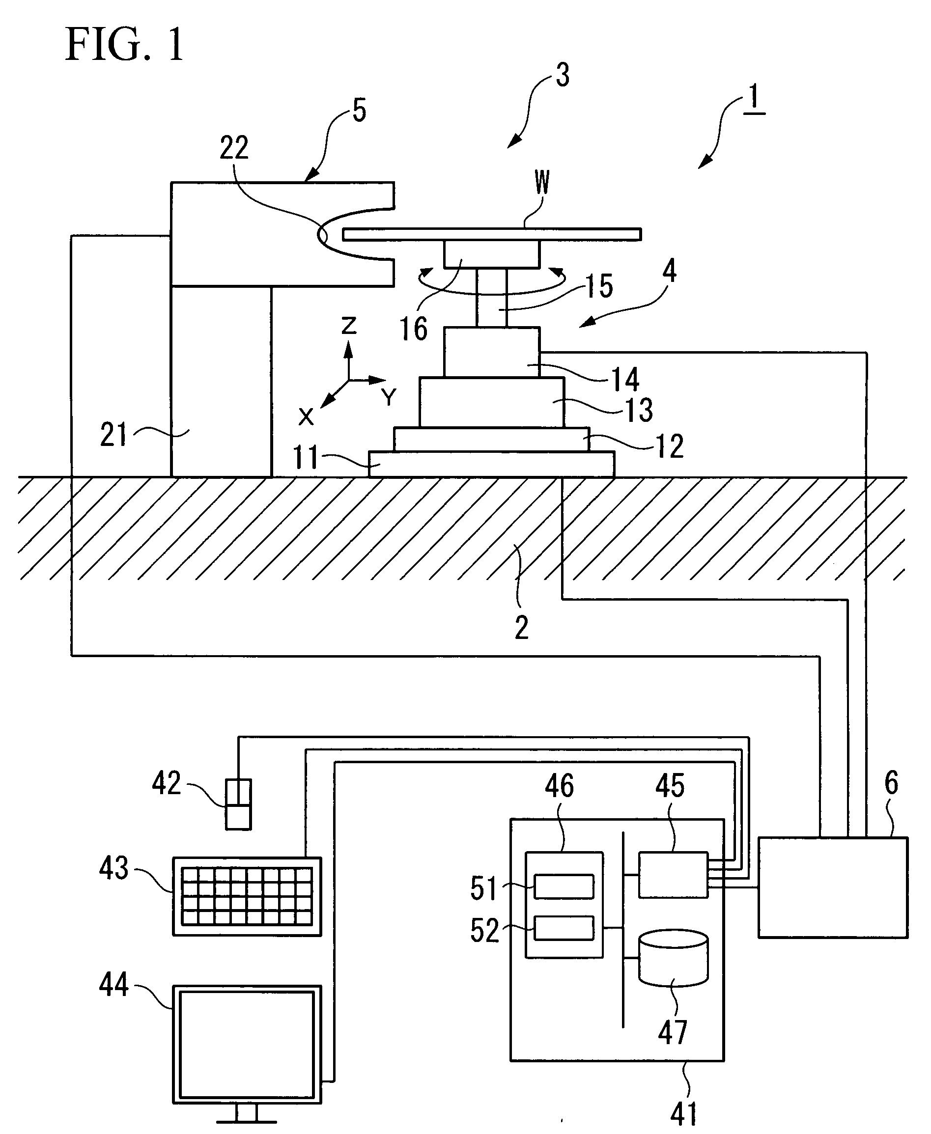
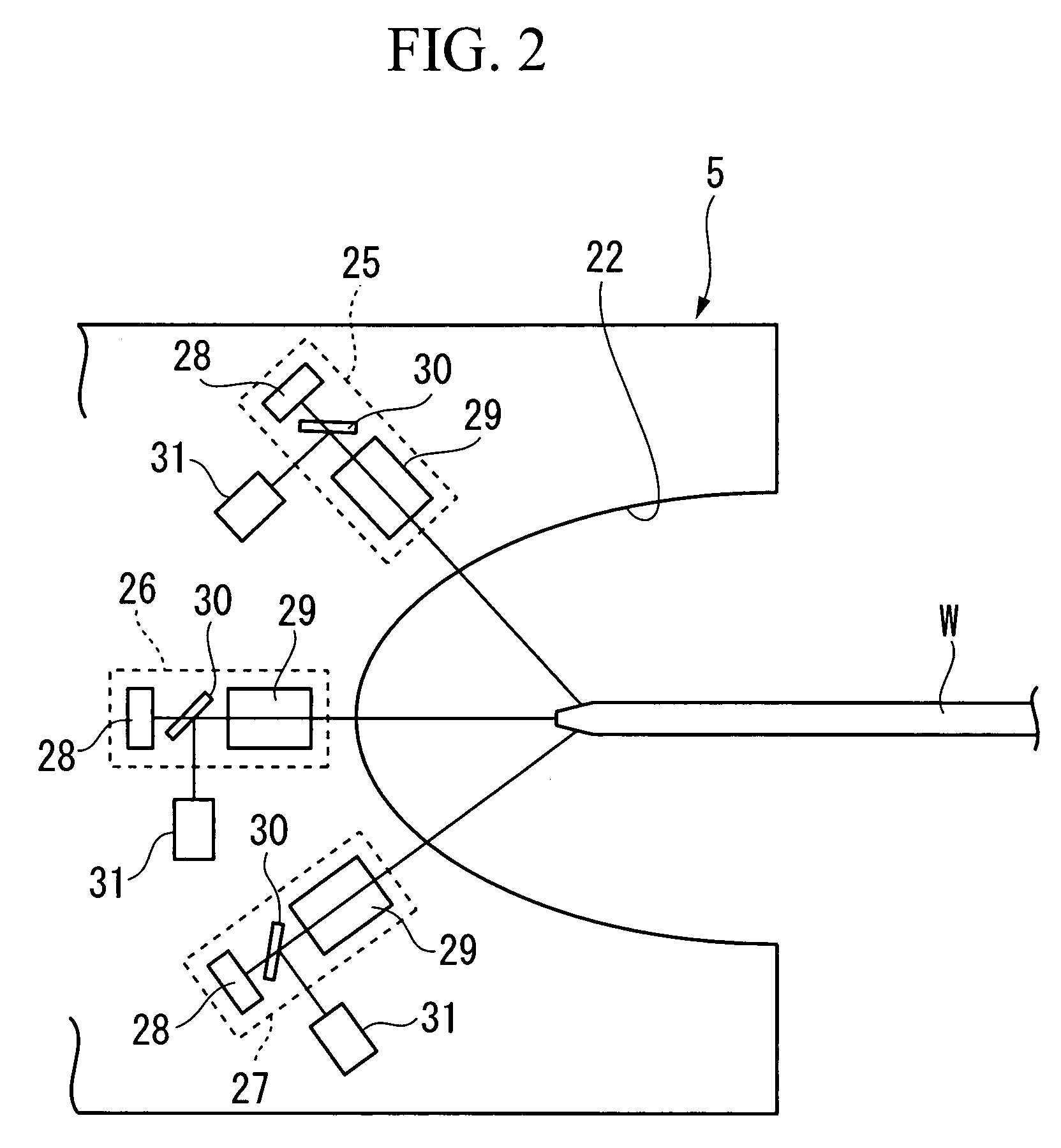
[0014]As shown in FIG. 1, a visual inspection apparatus 1 includes a base unit 2 fixed to a frame or the like not shown and an inspection unit 3 mounted an the base unit 2. The inspection unit 3 includes a wafer holder 4 on which a wafer W as an inspection target is placed and a peripheral edge imaging section 5 that is disposed close to the wafer holder 4 so as to acquire an image of a peripheral edge of the wafer W. The wafer holder 4 and the peripheral edge imaging section 5 are controlled by an apparatus control unit 6. A surface inspection section such as a microscope capable of observing the entire surface of the wafer W may be provided in addition to the peripheral edge imaging section 5.

[0015]The wafer holder 4 has an X stage 11 fixed to the base unit 2 so as to be movable in a horizontal direction indicated by X in FIG. 1. A Y stage 12 movable in the Y axis that is a horizontal direction perpendicular to the X axis is mounted on the X stage 11. A Z stage 13 movable in the Z...

second embodiment

[0038]A second embodiment of the invention is characterized in that an observation range or position can be automatically set on the basis of data registered in advance. The configuration of the visual inspection apparatus is similar to that of the first embodiment.

[0039]An example of the data registered in advance includes data indicating a position and a range of a wafer W grasped by a robotic arm for transporting the wafer W to the wafer holder 4. For example, as shown in FIG. 5, when a robotic arm 93 of a device 92 for transporting a wafer W from a wafer cassette 91 to the visual inspection apparatus 1 is of such a type to interpose the wafer W between two fixed holders 93A and 93B and one movable holder 93C, three holding portions W1 on which a force acts from the holders 93A to 93C. Since the holding portions W1 are contact portions with the grasping portions and portions on which an external force acts, chips or attachment of particles may easily occur in the holding portions...


PUM

PropertyMeasurementUnit
step angleaaaaaaaaaa

Abstract

The present invention is related to a visual inspection apparatus which can inspect a peripheral edge of a wafer with high efficiency. The visual inspection apparatus can make an inspection of any area on the peripheral edge of the wafer by displaying an inspection area specifying screen on a monitor. The inspection area specifying screen includes a display portion for displaying an observation range and an input portion for setting the observation area. The input portion allows one of step, continuity, and point to be selected as an observation type. A recipe is registered depending on a condition set in the above and thus is used to make an inspection.

Description

CROSS-REFERENCE TO RELATED APPLICATIONS[0001]This application claims priority from Japanese Patent Application No. 2006-268479, filed in the Japanese Patent Office on Sep. 29, 2006, the disclosure of which is incorporated herein by reference.BACKGROUND OF THE INVENTION[0002]1. Field of the Invention[0003]The present invention relates to an apparatus for inspecting a visual of a peripheral edge or the like of a substrate such as a wafer.[0004]2. Description of Related Art[0005]In semiconductor fabrication factories or the like, chips or cracks may be formed in the peripheral edges of semiconductor wafers. When such defects exist, they may cause damage to a wafer during manufacture. If a wafer is destroyed, damage occurs such that manufacturing apparatuses must be stopped for a long period of time, etc. Accordingly, a countermeasure has been taken in the recent fabrication factory of inspecting a peripheral edge of a wafer to check for defects such as chips formed during manufacturing...

Claims


Application Information

Patent Timeline
Patent Type & Authority Applications(United States)
IPC IPC(8): G01N21/00
CPCG01N21/9503
Inventor KOMURO, TAKAHIRO
Owner OLYMPUS CORP
Learn More